| Home | About Us | Contribute | Bookstore | Advertising | Subscribe for Free NOW! |
| News Archive | Features | Events | Recruitment | Directory |
Editor:
Mark Telford (Email)
Tel:+44 (0)1869 811577
Cell:+44 (0)7963 085605
Fax:+44 (0)1242 291482
Commercial Director /
Assistant Editor:
Darren Cummings (Email)
Tel:+44 (0)121 2880779
Cell:+44 (0)7990 623395
Fax:+44 (0)1242 291482
Advertisement Manager:
Jon Craxford (Email)
Tel:+44 (0)207 1939749
Cell:+44 (0)7989 558168
Fax:+44 (0)1242 291482
News
19 September 2006
First electrically pumped hybrid silicon laser
After demonstrating the first optically pumped hybrid silicon laser in November 2005, researchers at the University of California, Santa Barbara (UCSB) and Intel Corp have now demonstrated the world's first electrically pumped hybrid silicon laser using silicon manufacturing processes (full details to be published in the next issue of Optics Express journal).
The research team developed a method to combine the light-emitting and amplification properties of indium phosphide with the light-guiding capabilities of silicon into a single chip by bonding InP-based InGaAlAs optical gain layers directly to a silicon waveguide that forms the laser cavity and determines the laser's performance. Individual lasers can have different output wavelengths by simply modifying their silicon waveguide's properties without having to modify the InP-based material.
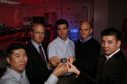
The UCSB and Intel hybrid silicon laser research team:
Hyundai Park, John Bowers, Mario Paniccia, Richard Jones, and Alexander
Fang.
The key to manufacturing the device is the use of a low-temperature, oxygen plasma to create a thin oxide layer (about 25 atoms thick) on the surfaces of both materials. The InP-based wafer is hence bonded directly to a pre patterned silicon photonic chip, eliminating the current need for slow and expensive aligning and attaching of discrete InP-based lasers to the silicon waveguide chip. When heated and pressed together the oxide layer functions as a 'glass-glue' fusing the two materials into a single chip. When a voltage is applied, light generated in the InP-based material couples directly through the oxide layer and into the silicon waveguide, where it is contained and controlled, creating a continuous laser beam that can be used to drive other silicon photonic devices. Being silicon-based, standard highvolume, lowcost silicon manufacturing techniques can be used to easily integrate the laser with other silicon photonic devices, producing highly integrated silicon photonic chips.
Also, compared to previous silicon Raman lasers, the hybrid silicon laser is an order of magnitude shorter (about 800 microns long; future generations will be significantly smaller). "We believe dozens, maybe even hundreds of hybrid silicon lasers could be created with a single bonding step and integrated with other silicon photonic components onto a single silicon chip," said Mario Paniccia, director of Intel's Photonics Technology Lab in Santa Clara.
"By combining UCSB's expertise with InP and Intel's silicon photonics expertise, we have demonstrated a novel laser structure based on a bonding method that can be used at the wafer-, partial-wafer or die-level, and could be a solution for large-scale optical integration onto a silicon platform," says UCSB professor of electrical and computer engineering John Bowers. While the use of comparable InP-based lasers is very expensive (from $50 to hundreds of dollars each), use of silicon could drastically reduce that cost to as little as a dollar per laser, the research team believes. "This marks the beginning of highly integrated silicon photonic chips that can be mass-produced at low cost," said Bowers.
Nahum Izhaky, photonics technology development manager at Intel's Jerusalem
R&D center and head of the Israeli team involved in the project, says the
technology allows data to be transferred from chip-to-chip via light. As the
demands of data transfer increase, the limitations of copper wiring on
transistors becomes ever more pressing. "We don't see limitations on the
transistors themselves, and it will take about 20 years to get there,"
Izhaky says. "The complications from using copper wiring in the
inter- connections between chips within the transistor however will limit our
capabilities in a few years' time, probably around 2012." The foreseeable
problems can be overcome with the current technology, but it would be very
complicated, inefficient and prohibitively expensive, he adds.
The hybrid silicon laser technology removes one of the last major barriers to producing low-cost, highly integrated, high-bandwidth silicon-based photonic chips for commun- ications between components inside and around PCs and servers, and between computers in data centers, says Paniccia. The fastest connections now send 8-10Gbit/s data signals over distances of up to 18 inches. With the new technology, speeds of 20-40Gbit/s could become common- place, over distances of tens of feet. Computer perfor- mance could increase sharply and hardware designs could change significantly (e.g. memory chips would no longer have to be kept close to microprocessor chips to reduce delays in fetching data). "This could enable low-cost, terabit optical 'data pipes' in future computers, making possible a flood of new applications for high-speed computing," adds Paniccia. "We now have all the building blocks."
With the proof of concept in place, the Jerusalem team can continue its work to bring it to the next stage of develop- ment in creating a suitable architecture, allowing the development of a commercial product. However, commer- cializing the technology could take at least five years. Initial test lasers stopped working at temperatures above about 100 degrees F, but the researchers believe they have identified ways to reduce the sensitivity to heat, adds Bowers.
*Talking exclusively to Semiconductor Today, Bowers added that UCSB has been working on the hybrid optical laser project for the past 18 months, spanning four generations of designs (the first two were optically pumped). The first ran pulsed and was the first demonstration of the concept, namely using a silicon waveguide and an evanescently coupled InGaAlAs gain region.
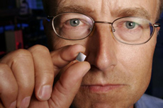
UCSB's John Bowers, professor of electrical and computer
engineering, with the hybrid silicon laser die.
Subsequently, a number of problems were fixed, namely smoother sidewalls
(fabricated in Intel's advanced CMOS process rather than UCSB's process) and
thicker oxide layers, both of which gave lower optical loss, and the lasers
ran continuous wave optically pumped.
UCSB then began the focus on electrical pumping, says Bowers. "Most people thought that the current would have to be extracted through the silicon layer; and the InP layer was too thin and hence too resistive. If you made the InP layer thicker to reduce the resistance, than the optical gain would be too low. We went through a number of design iterations, and came up with the third-generation: a pulsed electrically pumped laser. The design of the electrical structure is not simple, because the optical mode is sensitive to free-carrier absorption, so increasing the doping does not necessarily give lower threshold. The doping and composition of each layer are carefully designed to maximize the gain, and minimize the loss, heating and resistance."
Bowers adds that this latest, fourth generation contains an ion implant to
confine the current, and hence continuous wave operation has been achieved.
The next generation should increase the cw temperature from 40 C to 70 C,
Bowers predicts.
Visit:
http://www.intel.com
http://www.ece.ucsb.edu/uoeg
![]() ©2006 Juno Publishing and Media Solutions Ltd. All rights reserved. Semiconductor Today and the editorial material contained within it and related media is the copyright of Juno Publishing and Media Solutions Ltd. Reproduction in whole or part without permission from Juno Publishing and Media Solutions Ltd is forbidden. In most cases, permission will be granted, if the author, magazine and publisher are acknowledged.
©2006 Juno Publishing and Media Solutions Ltd. All rights reserved. Semiconductor Today and the editorial material contained within it and related media is the copyright of Juno Publishing and Media Solutions Ltd. Reproduction in whole or part without permission from Juno Publishing and Media Solutions Ltd is forbidden. In most cases, permission will be granted, if the author, magazine and publisher are acknowledged.
Disclaimer: Material published within Semiconductor Today and related media does not necessarily reflect the views of the publisher or staff. Juno Publishing and Media Solutions Ltd and its staff accept no responsibility for opinions expressed, editorial errors and damage/injury to property or persons as a result of material published.
Semiconductor Today, Juno Publishing and Media Solutions Ltd, Suite no. 133, 20 Winchcombe Street, Cheltenham, GL52 2LY, UK
Web site by No Name No Slogan ![]()