| Home | About Us | Contribute | Bookstore | Advertising | Subscribe for Free NOW! |
| News Archive | Features | Events | Recruitment | Directory |
| FREE subscription |
| Subscribe for free to receive each issue of Semiconductor Today magazine and weekly news brief. |
News
19 December 2008
Fujitsu develops CMOS logic-based 10V-breakdown transistor for PAs
At this week’s 2008 IEEE International Electron Devices Meeting (IEDM) in San Francisco, CA, USA, Japan’s Fujitsu Laboratories Ltd and Fujitsu Microelectronics Ltd reported the development of a high-voltage transistor (based on CMOS logic in silicon) that has a high breakdown voltage, suitable for power amplifiers used in wireless devices.
Fujitsu claims that it is the first 45nm-generation CMOS-based transistor capable of handling 10V power output, enabling it to handle high-output requirements necessary for power amplifiers used in WiMAX and other high-frequency applications.
The new technology enables power amplifiers to be formed on the same die as CMOS logic control circuitry to achieve single-chip integration, making high-performance, low-cost power amplifiers feasible, the firm claims.
Conventionally, due to the fact that power amplifiers for wireless devices need high power output at high frequencies, compound semiconductors such as gallium arsenide are mounted as a chip separate from control circuitry based on a general-purpose CMOS logic chip. If these chips' functions could be integrated onto a single chip, it would enable cost reduction of the overall module and likely speed the adoption of wireless devices to be used with wireless communication standards such as WiMAX and LTE (long-term evolution), says Fujitsu. The firm adds that there is hence a need for transistors that are compatible with CMOS logic process technology, and which can satisfy the requirements of power amplifiers necessary for WiMAX and other wireless communication standards.
However, the power output required of power amplifiers for use in high-frequency applications such as WiMAX exceeds the breakdown voltage of transistors used with standard CMOS logic processes. Overcoming this hurdle while remaining compatible with CMOS process technology therefore requires an increase in the transistor’s breakdown voltage. Since electric fields can lead to transistor failure, this is achieved by using a structure that lowers the electric field around the drain. Furthermore, structures with high breakdown voltages typically increase the transistor's on-resistance (the resistance between the transistor's source and drain when switched on), making it difficult to obtain satisfactory performance at high frequencies. Therefore, any solution would need to both raise breakdown voltage and avoid increasing on-resistance.
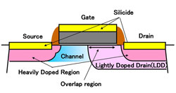 To overcome the above issues, Fujitsu says that it has developed a new transistor structure with the following characteristics (see Figure 1):
Figure 1: Structure of Fujitsu’s new transistor.
1. The transistor’s drain is surrounded by a lightly doped drain (LDD) region that overlaps with the gate. This lowers the electrical field extending horizontally to the drain as well as the electrical field extending to the gate oxide layer, raising the breakdown voltage.
2. The dopant distribution in the transistor channel follows a lateral gradient. This lowers the density of dopant on the drain side of the channel, limiting the increase in drain resistance (which is the main part of the on-resistance). It also lowers the electrical field extending horizontally to the drain, also raising the breakdown voltage.
The typical method for raising the breakdown voltage of a CMOS transistor has been to widen the gap separating the gate and the drain. The new structure suppresses on-resistance effectively compared to the conventional method, without increasing the gap.
 Furthermore, this new structure is believed to be highly compatible with standard transistors with 3.3V I/O circuitry, since it requires only the additional steps of forming the LDD region and the custom channel region.
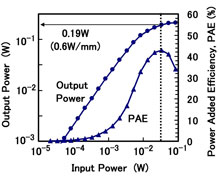
Figure 2: Characteristics of Fujitsu’s new power transistor (measured frequency: 2.1GHz; gate width: 0.32mm).
By using a 45nm process to apply the new transistor’s technology to standard transistors with 3.3V I/O, Fujitsu reckons that it has developed the world's first transistor to raise the breakdown voltage from 6V to 10V. Regarding features that make the new transistor suitable for use in power amplifiers, power output of 0.6W per gate width of 1mm (0.6W/mm) was reached at a maximum oscillation frequency of 43GHz (Figure 2), demonstrating sufficient performance for use as a power transistor in WiMAX. The new transistor also produced good results in basic reliability testing, the firm adds.
Fujitsu reckons that its new high-voltage transistor technology paves the way for CMOS logic-based transistors with high breakdown voltages to be used in power amplifiers. The firm aims to develop the technology further, targeting the single-chip integration of power amplifiers and control circuitry, in order to realize low-cost high-performance power amplifier modules.
See related items:
Fujitsu reports record-performance 5GHz-bandwidth hybrid amplifier
Fujitsu reports record 320W C-band power amplifiers
Fujitsu claims first high-output GaN HEMT to cut power in standby mode
![]() Search: Fujitsu CMOS logic transistor
Search: Fujitsu CMOS logic transistor
Visit: http://jp.fujitsu.com/group/labs/en
![]() ©2008 Juno Publishing and Media Solutions Ltd. All rights reserved. Semiconductor Today and the editorial material contained within it and related media is the copyright of Juno Publishing and Media Solutions Ltd. Reproduction in whole or part without permission from Juno Publishing and Media Solutions Ltd is forbidden. In most cases, permission will be granted, if the author, magazine and publisher are acknowledged.
©2008 Juno Publishing and Media Solutions Ltd. All rights reserved. Semiconductor Today and the editorial material contained within it and related media is the copyright of Juno Publishing and Media Solutions Ltd. Reproduction in whole or part without permission from Juno Publishing and Media Solutions Ltd is forbidden. In most cases, permission will be granted, if the author, magazine and publisher are acknowledged.
Disclaimer: Material published within Semiconductor Today and related media does not necessarily reflect the views of the publisher or staff. Juno Publishing and Media Solutions Ltd and its staff accept no responsibility for opinions expressed, editorial errors and damage/injury to property or persons as a result of material published.
Semiconductor Today, Juno Publishing and Media Solutions Ltd, Suite no. 133, 20 Winchcombe Street, Cheltenham, GL52 2LY, UK
Web site by No Name No Slogan ![]()