| Home | About Us | Contribute | Bookstore | Advertising | Subscribe for Free NOW! |
| News Archive | Features | Events | Recruitment | Directory |
| FREE subscription |
| Subscribe for free to receive each issue of Semiconductor Today magazine and weekly news brief. |
News
10 October 2008
Fujitsu claims first high-output GaN HEMT to cut power in standby mode
At the International Symposium on Compound Semiconductors (ISCS) in Rust, Germany (21-24 September), Tokyo-based Fujitsu Ltd and Fujitsu Laboratories Ltd presented what is claimed to be the first gallium nitride (GaN)-based high-electron-mobility transistor (HEMT) with a structure that achieves high output of over 100W while also enabling power to be cut when the device is in standby mode. Fujitsu says that the advance should contribute to higher output and lower power consumption in amplifiers for high-speed wireless communications at microwave (30MHz to 30GHz) and millimeter-wave (30-300GHz) frequencies (for which usage is expected to grow).
As transmission speeds in next-generation wireless communications have increased, wireless base-stations that operate in the microwave frequency range at several gigahertz consume an ever-increasing amount of power. In addition to the fact that the millimeter-wave frequency range above 30GHz has a large amount of available bandwidth that is currently unused, its potential for use in high-speed transmissions is significant since it delivers high speed and good directionality, says Fujitsu. However, because millimeter-wave frequencies are higher than frequencies used for conventional wireless transmissions, it has been difficult to develop amplifiers for practical use that are both compact and economical, so the millimeter band has so far not been widely used.
Amplifiers based on silicon have low breakdown voltages, making it difficult for them to achieve both high frequencies and high power output, so attention has shifted to compound semiconductors with higher breakdown voltages. GaN-based compounds have high innately high breakdown voltages, suiting high-output applications. The development of high-output power amplifiers enables microwave and millimeter-wave transmissions to be used in high-speed wireless communications.
Previous amplifiers based on compound semiconductors have required a negative voltage to be applied continuously to the gate electrode (see Figure 1a) even when the circuit is in standby mode (enabling the electron density just below the gate to be zero, allowing the transistor's current flow to be turned off). This results in high power consumption. Until now, no compound semiconductor transistor had been able to both generate 100W of power output and cut power consumption without requiring the addition of a negative voltage. Also, because the design of the control circuits used in previous transistors has been very complex, they required more power to be consumed.
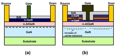
Figure 1: GaN HEMT: (a) conventional structure; (b) structure of Fujitsu's new HEMT.
Figure 1b shows the structure of Fujitsu’s new GaN HEMT transistor, which it claims is the first that does not require a negative voltage to turn off the circuit's power. Key features include the following:
- The addition of an aluminium nitride (AlN) layer on top of the n-type GaN layer increases the density of charge carriers in the two-dimensional electron gas on the GaN side of the GaN/n-AlGaN interface when the transistor is switched on. In a HEMT transistor, a high electron density makes the design naturally amenable to higher power output.
- The design of the gate electrode, formed after removing the AlN layer, decreases the density of carrier electrons in the region below the gate electrode, preventing current from flowing even in the absence of a negative voltage.
- Making the topmost layer from AlN results in a micro-cracked surface (see Figure 2a), which degrades the breakdown voltage. So, an n-type GaN-based top layer was added, resulting in a three-layer cap structure that improves the surface roughness (see Figure 2b) as well as raising output and reliability.
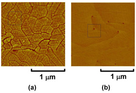 Figure 2: Atomic-scale surface roughness on GaN HEMT: (a) two-layer cap structure without uppermost layer; (b) new three-layer cap structure.
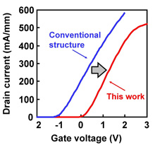 Figure 3: Carrier transfer characteristics.
The new three-layer cap structure obviates the need for a negative voltage across the gate electrode and results in a GaN HEMT that allows power to be cut during standby. Fujitsu also verified that the addition of the AlN layer increases the volume of electrons transmitted by 60% (Figure 1b). This results in the transistor's characteristic of being able to sustain high current densities when on, but cut power when on standby (see Figure 3).
The three-layer structure permits breakdown voltages exceeding 300V, resulting in what Fujitsu claims is an unprecedented combination of achieving high current densities and high breakdown voltages (see Figure 4). This enables high-efficiency power amplification with low resistance and low power consumption. Implementation of the new transistor structure eliminates the need for power during standby, and has realized output exceeding 100W (the first time that both have been achieved simultaneously, claims the firm).
Fujitsu says that it aims to pursue commercialization of the GaN transistor technology, aiming to apply it in high-capacity wireless communications systems by about 2010.
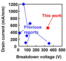
Figure 4: Maximum drain current and breakdown voltage benchmarks (enabling current to be turned off without applying a negative voltage).
Aspects of the research were conducted as part of the Research and Development Project for Expansion of Radio Spectrum Resources, sponsored by Japan’s Ministry of Internal Affairs and Communications.
See related items:
Fujitsu develops first impulse radio transmitting at over 10Gb/s in millimeter band
Fujitsu’s GaN HEMT-based mobile WiMAX base-station chosen by UQ
Fujitsu launches GaN HEMT-based mobile WiMAX base-stations
Search: Fujitsu Laboratories GaN HEMT AlN
Visit: www.fujitsu.com
![]()
![]() ©2008 Juno Publishing and Media Solutions Ltd. All rights reserved. Semiconductor Today and the editorial material contained within it and related media is the copyright of Juno Publishing and Media Solutions Ltd. Reproduction in whole or part without permission from Juno Publishing and Media Solutions Ltd is forbidden. In most cases, permission will be granted, if the author, magazine and publisher are acknowledged.
©2008 Juno Publishing and Media Solutions Ltd. All rights reserved. Semiconductor Today and the editorial material contained within it and related media is the copyright of Juno Publishing and Media Solutions Ltd. Reproduction in whole or part without permission from Juno Publishing and Media Solutions Ltd is forbidden. In most cases, permission will be granted, if the author, magazine and publisher are acknowledged.
Disclaimer: Material published within Semiconductor Today and related media does not necessarily reflect the views of the publisher or staff. Juno Publishing and Media Solutions Ltd and its staff accept no responsibility for opinions expressed, editorial errors and damage/injury to property or persons as a result of material published.
Semiconductor Today, Juno Publishing and Media Solutions Ltd, Suite no. 133, 20 Winchcombe Street, Cheltenham, GL52 2LY, UK
Web site by No Name No Slogan ![]()