| Home | About Us | Contribute | Bookstore | Advertising | Subscribe for Free NOW! |
| News Archive | Features | Events | Recruitment | Directory |
CMP PROCESSING
Learn more about R&D chemical mechanical polishing by requesting our FREE informational CD.

| FREE subscription |
| Subscribe for free to receive each issue of Semiconductor Today magazine and weekly news brief. |
News
7 January 2008
FBH orders WEP CVP21 wafer ECV-profiler
WEP (Wolff für Elektronik- und Programmentwicklungen) of Furtwangen im Schwarzwald, Germany has received an order from the Ferdinand-Braun-Institut für Höchstfrequenztechnik (FBH) for a Wafer ECV-Profiler CVP21. The profiler will be installed in an FBH clean room close to the organisation’s nitride growth equipment.
Thomas Wolff, president of WEP, said: “The CVP21 is an advanced equipment to monitor the quality of semiconductor layers and includes comprehensive self-calibration algorithms to achieve results with high reliability. Ferdinand-Braun-Institut is recognized for its profound knowledge in the field of ECV profiling and WEP is proud to support this prestigious institution in the development of exciting new devices in the field of microwave electronics and optoelectronics.”
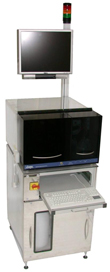 A fully automated system for carrier concentration profiling, the CVP21 automates the entire measurement process, including automated fluid handling, automated movement of the electrochemical cell, automated in-situ imaging and automated CV scan analysis to produce reproducible measurement results with high accuracy. It contains a patented process for the processing of (Al,In)GaN samples in full-automation mode.
The CVP21 has a footprint of 60(W) x 80(D) x 195(H)cm, and is also available as a table-top unit.
As well as its CVP21 wafer profiler, WEP offers process control systems and software.
Picture: CVP21 electrochemical CV wafer profiler from WEP.
See related item:
Institute of Semiconductor Technology, University of Braunschweig orders CV wafer profiler from WEP
Visit: www.wepcontrol.com/cv-profiler
Visit: www.fbh-berlin.de
![]()
![]() ©2008 Juno Publishing and Media Solutions Ltd. All rights reserved. Semiconductor Today and the editorial material contained within it and related media is the copyright of Juno Publishing and Media Solutions Ltd. Reproduction in whole or part without permission from Juno Publishing and Media Solutions Ltd is forbidden. In most cases, permission will be granted, if the author, magazine and publisher are acknowledged.
©2008 Juno Publishing and Media Solutions Ltd. All rights reserved. Semiconductor Today and the editorial material contained within it and related media is the copyright of Juno Publishing and Media Solutions Ltd. Reproduction in whole or part without permission from Juno Publishing and Media Solutions Ltd is forbidden. In most cases, permission will be granted, if the author, magazine and publisher are acknowledged.
Disclaimer: Material published within Semiconductor Today and related media does not necessarily reflect the views of the publisher or staff. Juno Publishing and Media Solutions Ltd and its staff accept no responsibility for opinions expressed, editorial errors and damage/injury to property or persons as a result of material published.
Semiconductor Today, Juno Publishing and Media Solutions Ltd, Suite no. 133, 20 Winchcombe Street, Cheltenham, GL52 2LY, UK
Web site by No Name No Slogan ![]()