| Home | About Us | Contribute | Bookstore | Advertising | Subscribe for Free NOW! |
| News Archive | Features | Events | Recruitment | Directory |
| FREE subscription |
| Subscribe for free to receive each issue of Semiconductor Today magazine and weekly news brief. |
News
21 July 2008
Step towards low-cost white light emitters with back-reflectors
Researchers at Purdue University in West Lafayette, IN, USA have developed a stack of materials on silicon that could lead to more efficient, lower-cost gallium nitride (GaN) light-emitting devices [Oliver et al, App. Phys. Lett., vol.93, p023109, 2008]. The stack includes a light-reflecting conductive layer that would boost light output from devices and provide an ohmic back-contact for the diode structure.
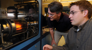
Picture: Timothy D. Sands (left), director of Purdue's Birck Nanotechnology Center in
Discovery Park, and graduate student Mark Oliver, operate a reactor. Inside
the reactor, GaN is deposited on silicon with an integrated ZrN
back-reflector at temperatures of about 1000C. (Purdue News Service
photo/David Umberger)
White-light LEDs promise efficient long-lasting light sources – four times the efficiency of incandescent lights (~10%) with life-times of up to 15 years. White LEDs are also seen as more environmentally friendly compared with compact fluorescents that contain mercury. It is estimated that one-third of the electrical power consumed in the USA is used for lighting. White LED-based lighting presently costs about $100 but, for significant market penetration, this must be reduced to about $5.
Currently, light-emitting GaN devices are predominantly produced on sapphire or silicon carbide substrates, depending on considerations of cost or power output. Sapphire was the first material on which GaN was grown to produce commercial LEDs, but the large lattice mismatch between the materials (of about 14%) leads to the GaN surface containing a large number of defects that impact device production yields, efficiencies and life-times. SiC substrates have a lesser mismatch (~3%) and better thermal conductivity, but are much more expensive to produce. Single-crystal bulk GaN is prohibitively expensive to make. ‘Free-standing’ GaN is often produced on, and then separated from, one of the traditional substrates (sapphire or SiC).
From a cost perspective, silicon (Si) has the advantage of being lower cost than sapphire, both in terms of raw materials and from the economies of scale that can be achieved with using larger-diameter wafers – presently at 300mm and threatening to go to 450mm, compared with sapphire’s 100mm. Silicon also has better thermal conductivity compared with sapphire (although not with SiC).
The main disadvantage of silicon is that it has an even greater lattice mismatch (of about 20%). Even so, some companies, such as Nitronex in the USA, have developed GaN/Si substrates for producing high-frequency RF transistors in volume. Others, such as Shimei Semiconductor in Japan, are developing GaN/Si LEDs, but there do not seem to be any products available as yet.
The Purdue stack bridges the GaN-Si lattice mismatch with two layers, of aluminum nitride (AlN) and zirconium nitride (ZrN). The AlN provides a barrier between the Si and ZrN layers. Without the AlN, ZrN and Si react, producing SiN and ZrSi, at the high temperatures that are used in the metal-organic chemical vapor deposition (MOCVD)/organo-metal vapor phase epitaxy (OMVPE) processes used for GaN deposition (of more than 1000C). While molecular beam epitaxy (MBE) deposition can be performed at lower temperatures (of about 600C), the process is more time consuming and difficult to apply in mass production. Such Si-ZrN reactions lead to opaque GaN layers and blistering. Opacity is clearly not desirable in a light-emitting product.
Added advantages of using an AlN barrier are the relatively high thermal conductivity of the material and the electrical insulation that it could provide between devices on the same die emitting at different wavelengths. The ZrN layer could also be used in a lattice-matched form with green-light-emitting In0.14Ga0.86N.
The ZrN/AlN/Si stack was produced by using dc magnetron sputtering to first deposit a thin layer of Al metal to protect the silicon from nitridation. An argon-nitrogen gas mixture is then used to convert the Al to AlN. This was followed by further AlN deposition and then the ZrN layer. Various ranges of layer thicknesses were investigate: 80450nm for the AlN and 70300nm for the ZrN. The deposition speeds were of the order of 60nm/hr for AlN and 80nm/hr for ZrN. A thin (~3nm) AlN capping layer was deposited to protect the ZrN from oxidation. The cap is also thought to reduce the ZrN/GaN contact resistance by lowering the effective barrier between the materials.
The 2002000nm GaN layer was deposited using OMVPE at temperatures of up to 1020C. Much of the Purdue paper is devoted to measuring the crystal quality of the various layers using x-ray diffraction. The sharpness of the various diffraction peaks, as derived by ‘rocking’ the material in various directions, gives an indication of the crystal quality – the narrower the curve, the better the crystal. Excluding the Si substrate, which has very narrow peaks due to its highly crystalline nature, the crystal quality improves between the AlN up to the GaN layer. For example, the ‘omega’ rocking curve for 0002 reflection gives full-widths at half maximum (FWHMs) for a 115nm AlN layer of 1.7degrees, 1.3degrees and 0.4degrees (1430arcsecs), respectively, for 115nm AlN, 80nm ZrN and 860nm GaN stacks. By comparison, commercial GaN-on-sapphire rocking curves have FWHMs of a few hundreds of arcseconds (100arcsec=0.025degrees).
The Purdue team comments that their results open up the way to cost reduction and the scale-up of discrete LEDs and integrated LED arrays with back reflectors, but that there remain a number of challenges that require further work. One such challenge is the 35% difference in thermal expansion between the GaN layer and the silicon substrate. This leads to cracking as the stack is cooled when the GaN layer is greater than 1000nm. A separate problem is that the GaN layer on top of the ZrN/AlN/Si shows a high threading dislocation density.
The leader of the research, professor Timothy D. Sands, comments: “These are engineering issues, not major show stoppers. The major obstacle was coming up with a substrate based on silicon that also has a reflective surface underneath the epitaxial gallium nitride layer, and we have now solved this problem.”
Sands expects these issues to met by industry. He also sees affordable white LED lighting becoming available within the next two years.
See related item:
Compound semiconductor substrate market to top $1bn by 2009-2010
Search: White LEDs GaN GaN-on-Si SiC substrates Sapphire substrates AlN
Visit: https://engineering.purdue.edu/HetInt
The author Mike Cooke is a freelance technology journalist who has worked in the semiconductor and advanced technology sectors since 1997.
![]()
![]() ©2008 Juno Publishing and Media Solutions Ltd. All rights reserved. Semiconductor Today and the editorial material contained within it and related media is the copyright of Juno Publishing and Media Solutions Ltd. Reproduction in whole or part without permission from Juno Publishing and Media Solutions Ltd is forbidden. In most cases, permission will be granted, if the author, magazine and publisher are acknowledged.
©2008 Juno Publishing and Media Solutions Ltd. All rights reserved. Semiconductor Today and the editorial material contained within it and related media is the copyright of Juno Publishing and Media Solutions Ltd. Reproduction in whole or part without permission from Juno Publishing and Media Solutions Ltd is forbidden. In most cases, permission will be granted, if the author, magazine and publisher are acknowledged.
Disclaimer: Material published within Semiconductor Today and related media does not necessarily reflect the views of the publisher or staff. Juno Publishing and Media Solutions Ltd and its staff accept no responsibility for opinions expressed, editorial errors and damage/injury to property or persons as a result of material published.
Semiconductor Today, Juno Publishing and Media Solutions Ltd, Suite no. 133, 20 Winchcombe Street, Cheltenham, GL52 2LY, UK
Web site by No Name No Slogan ![]()