| Home | About Us | Contribute | Bookstore | Advertising | Subscribe for Free NOW! |
| News Archive | Features | Events | Recruitment | Directory |
| FREE subscription |
| Subscribe for free to receive each issue of Semiconductor Today magazine and weekly news brief. |
News
11 March 2008
EMF announces multiple MOCVD orders
EMF Semiconductor Systems Ltd of Mitchelstown, Ireland says that it sold multiple MOCVD systems in fourth-quarter 2007.
Last November, co-funded by both South Africa’s National Research Foundation, Nelson Mandela Metropolitan University bought a Mercury single-wafer MOCVD system for the development of nanostructures for photonic applications. The university’s Physics department, which has been involved in MOCVD growth since the mid-1980s, already has two MOCVD reactors dedicated to R&D of both III-V and II-VI materials. However, this latest reactor, scheduled for delivery in Q3/2008, is a significant upgrade to the current tools and will allow far greater flexibility and control over the growth process.
 “The Mercury tool will profoundly change the productivity of their department and even allow them to begin commercializing their process,” says EMF’s technical sales manager, Dr Matthew Branch. “Whereas reproducibility was limited for them in the past, the Mercury tool offers a complete package with a state-of-the-art control console and proven system performance”.
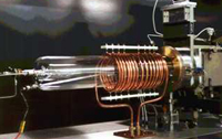
Picture (above): EMF Semiconductor's Mercury MOCVD tool.
 Also, in December, an unnamed telecom company in Islamabad, Pakistan placed an order for a Titan multi-wafer MOCVD tool, to be delivered in December 2008 and fully configured for both narrow- and wide-bandgap materials including GaN.
Picture (left): EMF Semiconductor's Titan MOCVD tool.
The Titan is one of EMF’s ‘next-generation’ tools, incorporating the patented Vectored-Flow Epitaxy (VFE) process, which involves separate injection of each of the process reagents into the growth chamber and - more importantly – maintaining their separation in the gas phase. The quasi-atomic layer deposition process prevents harmful pre-reactions between incompatible reagents, improving crystal quality and reducing expensive reagent consumption, claims EMF. The tool has also generated significant interest in recent months for ZnO-type applications, the firm adds.
Finally, following the recent success in jointly developing a commercial-scale remote-plasma chemical vapor deposition (RPCVD) process with Australia’s BluGlass Ltd for the manufacture of GaN-based blue LEDs, a second tool, for R&D purposes, is being manufactured, and is on track for delivery in 2008. The patented RPCVD process for growing nitride materials at low temperatures also shows promise for applications such as oxide-nitride mixed structures, photovoltaics and silicon. Combined with EMF technology, the R&D tool offers a complete package that has received considerable interest from universities, research institutes and companies worldwide, says EMF.
See related items:
BluGlass makes its first quantum well LEDs
BluGlass awards first equipment manufacturing contract
Search: EMF Semiconductor MOCVD
Visit: www.emfsemi.com