
| Home | About Us | Contribute | Bookstore | Advertising | Subscribe for Free NOW! |
| News Archive | Features | Events | Recruitment | Directory |
| FREE subscription |
| Subscribe for free to receive each issue of Semiconductor Today magazine and weekly news brief. |
News
16 January 2009
SMI opens applications lab for MOCVD of ZnO-based films
Structured Materials Industries Inc (SMI) of Piscataway, NJ, USA, which provides metal-organic chemical vapor deposition (MOCVD) systems, components, materials, and process development services, has opened its application lab facilities for the MOCVD growth of ZnO-based films for transparent contacts, as used with LEDs and photovoltaics, as well as ZnO films for transparent and power transistors.
SMI has a decades-long history of developing zinc oxide and its alloys and has built capabilities in its in-house applications lab, including four ZnO deposition tools, thermal and laser annealing stations, and other support services. The tools are used predominantly in support of customer development needs and deposition tool purchasers.
In-house tools include platters with sizes of 5-12”. Materials properties include n-type conductors doped to a concentration of 10E20 with conductivities as low as 5E-4 ohm-cm, or insulating films with conductivities greater than 10E7 ohm-cm. SMI says that it has experience with a wide range of dopants for tuning the energy bandgap, the index of refraction, and the conductivity. Also available are p-type exploration services.
Deposition services include demonstrated development of alloys of ZnO (Cd, Mg, Se, Te, and S), doping of ZnO (In, Ga, Al, B, N, P, As, Li, Na, K, and Sb, among others) and phosphor or spin materials compositions (Cu, Fe, Co, Mn, Si, Ge, Er, Nb, Eu, and Tb, among others).
 Application areas include gallium nitride (GaN) LEDs, especially UV LEDs, where only ZnO alloys will effectively allow ultraviolet light out while maintaining conductivity.
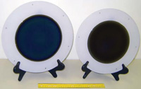
Picture: SMI-MOCVD-grown ZnO thin films (conductive or insulating) through 8”, now routinely produced with less than 3% uniformity.
SMI says that ZnO conductors are applicable to cadmium telluride (CdTe) and copper indium gallium diselenide (CIGS) photovoltaics. As well as being used in conventional LEDs, ZnO (or its alloys) can also be used as a phosphor layer in a device structure, e.g. in white LEDs.
In addition, ZnO nanowire structures have great potential as sensors and possibly even a new type of laser, says SMI.
See related items:
SMI licenses SiC MOCVD technology from Veeco
![]() Search: SMI MOCVD ZnO GaN CdTe CIGS
Search: SMI MOCVD ZnO GaN CdTe CIGS
Visit: www.structuredmaterials.com

![]() ©2009 Juno Publishing and Media Solutions Ltd. All rights reserved. Semiconductor Today and the editorial material contained within it and related media is the copyright of Juno Publishing and Media Solutions Ltd. Reproduction in whole or part without permission from Juno Publishing and Media Solutions Ltd is forbidden. In most cases, permission will be granted, if the author, magazine and publisher are acknowledged.
©2009 Juno Publishing and Media Solutions Ltd. All rights reserved. Semiconductor Today and the editorial material contained within it and related media is the copyright of Juno Publishing and Media Solutions Ltd. Reproduction in whole or part without permission from Juno Publishing and Media Solutions Ltd is forbidden. In most cases, permission will be granted, if the author, magazine and publisher are acknowledged.
Disclaimer: Material published within Semiconductor Today and related media does not necessarily reflect the views of the publisher or staff. Juno Publishing and Media Solutions Ltd and its staff accept no responsibility for opinions expressed, editorial errors and damage/injury to property or persons as a result of material published.
Semiconductor Today, Juno Publishing and Media Solutions Ltd, Suite no. 133, 20 Winchcombe Street, Cheltenham, GL52 2LY, UK
Web site by No Name No Slogan ![]()