- News
6 December 2010
AlGaN-channel with more than 50% Al achieves 1800V breakdown
Researchers at University of Fukui, Sharp Corp and Sumitomo Electric Industries Ltd have produced high-electron-mobility transistors (HEMTs) with aluminum gallium nitride (AlGaN) channels with Al content of more than 50% for the first time [Hirokuni Tokuda et al, Appl. Phys. Express, vol3, p121003, 2010]. The team is aiming to produce higher-power semiconductor devices. The new devices achieved a breakdown voltage of 1800V, which is the highest value reported so far among AlGaN-channel HEMTs, according to the researchers.
HEMT devices using the conducting electron sheet (two-dimensional electron gas) formed at the interface between an AlGaN barrier and GaN channel have variously achieved power densities of 32.2W/mm in the C band (4–8GHz) and maximum oscillation frequencies of up to 300GHz. Such performance characteristics are of great interest for microwave and millimeter-wave applications (communications, radar, etc).
High-power applications for nitride semiconductor devices have recently come to prominence, for example with companies developing inverter systems (DC-to-AC conversion) for hybrid electric vehicles and for renewable energy (solar, wind) plumbing into a smart electric power grid. These devices need to have high breakdown voltage and may need to operate at high temperature.
HEMTs with AlGaN channels have been proposed as providing a way to achieve these properties. These devices have a wider bandgap of AlGaN compared with GaN. A wider bandgap is generally associated with both higher breakdown electric fields and an ability to operate at higher temperature. However, high-Al-content AlGaN is difficult to grow with high quality on traditional substrates.
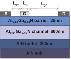 The researchers used free-standing single-crystal c-plane aluminum nitride (AlN) pieces as the substrate, typically measuring 10mm x 10mm. The substrate material was chosen in order to allow better epitaxial growth quality for the high-Al-content AlGaN layers. AlN has a smaller lattice mismatch with such high-Al-content layers, compared with more traditional substrate materials such as silicon carbide and sapphire. Metal-organic chemical vapor deposition (MOCVD) was used as the epitaxial growth technique (Figure 1). None of the layers of the AlGaN-channel HEMT were intentionally doped.
Figure 1: Schematic cross-section of fabricated AlGaN-channel HEMT.
Since suitable ohmic contacts were not obtained using traditional titanium/aluminum stacks, the researchers employed a recently developed system combining zirconium, aluminum, molybdenum and gold (Zr/Al/Mo/Au, 15/60/35/50nm). The stack was processed with a 950ºC anneal for 30secs.
The Schottky gate contact consisted of nickel-gold. The gate length was 9μm. The gate-source spacing was 3μm. The widths of the devices were 515μm. The gate–drain distance was varied between 5μm and 15μm, allowing the breakdown voltage variation with this parameter to be studied. A comparison device consisted of an Al0.25Ga0.75N/GaN (GaN-channel) HEMT produced on silicon.
An AlGaN-channel HEMT with gate–drain distance of 10μm had a maximum drain current of 13.0mA (25.2mA/mm) at a drain voltage of 50V. The drain saturation current (i.e. at zero gate voltage) was 4.7mA (9.1mA/mm). The maximum transconductance was 2.4mS (4.7mS/mm). The threshold for pinch-off was –5.5V.
The current and transconductance were smaller than previous AlGaN-channel HEMTs (with lower Al contents) reported in 2007–2008. This is attributed to a high channel resistance. Room-temperature transmission line model measurements gave an ohmic specific contact resistance of 4.8x10⁻²Ω-cm2. The sheet resistance was found to be 2900Ω/sq. C–V profiling was used to estimate the electron concentration at the barrier/channel interface, giving a value of about 5x10¹⁹/cm2.
Since the channel resistance is relatively high, the researchers believe that this is caused by low mobility of the AlGaN material. However, this cannot be confirmed directly by Hall measurements since the sample size is too small. The researchers comment: ‘Further work is needed to improve epitaxial layer quality and structure, such as introducing a low-resistive cap layer.’
The breakdown voltage grew linearly with the gate–drain distance, reaching 1800V for 15μm gate–drain devices. These experiments were carried out at gate voltage –20V, giving a fully pinched-off channel. The breakdown of 1800V compares with a value of 1650V achieved by Mitsubishi using an Al0.38Ga0.62N channel.
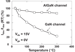 The Fukui–Sharp–Sumitomo researchers also found that the AlGaN-channel device maintained its saturation drain current performance more effectively at high temperature than the GaN-channel comparison (Figure 2). The fall in current over the range from room temperature to 300°C for the AlGaN-channel device was 20%. The GaN-channel comparison device current fell 80% over the same range.
Figure 2: Temperature dependence of drain saturation current. Current is normalized at room temperature. Square and circle symbols are obtained from the developed AlGaN-channel and conventional GaN-channel HEMT, respectively.
Given the long gate length, the researchers see this as reflecting the temperature dependence of the channel electron mobilities of the respective devices. Further investigation would require studying devices with different gate lengths at varying temperatures, the researchers comment.
‘The temperature-insensitive characteristic of AlGaN-channel HEMT is a great advantage for stable high-temperature device operation in many practical applications,’ the researchers add.
The contact resistance also decreased as the temperature increased to 300°C, falling to 1.5x10⁻²Ω-cm2 for the AlGaN-channel device. The GaN-channel device also benefitted from this effect – the contact resistance at room temperature was 6x10⁻⁶Ω-cm2 at room temperature and 5.8x10⁻⁷Ω-cm2 at 300°C.
Nitride HEMT on silicon achieves 143GHz current gain cut-off frequency
Fluoride push to nitride HEMT enhancement
The author Mike Cooke is a freelance technology journalist who has worked in the semiconductor and advanced technology sectors since 1997.