| Home | About Us | Contribute | Bookstore | Advertising | Subscribe for Free NOW! |
| News Archive | Features | Events | Recruitment | Directory |
News
10 September 2010
Nitride HEMT on silicon achieves 143GHz current gain cut-off frequency
Researchers based in Switzerland have enhanced the high-frequency performance of nitride-based high-electron-mobility transistors (HEMTs) grown on silicon substrates [Haifeng Sun et al, Appl. Phys. Express, vol3, p094101, 2010]. The researchers, based at ETH-Zürich and Ecole Polytechnique Fédérale de Lausanne (EPFL), created HEMTs with current gain (fT) and maximum oscillation (fMAX(U)) cutoff frequencies of 143 GHz and 176 GHz, respectively.
The previous record for nitride HEMTs grown on high-resistivity (HR) silicon gave an fT of 107 GHz and an fMAX(U) of 150 GHz. The new Swiss HEMTs used a structure with barriers made of aluminum indium nitride (AlInN) rather than the more traditional aluminum gallium nitride (AlGaN). A number of applications in the past few months have made use of high quality AlInN growth methodologies that have recently become available. One advantange of AlInN is that is can be lattice matched to the underlying GaN, in principle reducing strain-related reliability problems. AlGaN cannot be lattice matched to GaN.
Nitride HEMTs are attractive for power amplification of radio signals, such as for base-station transmissions from wireless networks. However, such devices are generally grown on expensive substrates such as silicon carbide to achieve high-frequency performance. For example, AlGaN/GaN and AlInN/GaN HEMTs on semi-insulating silicon carbide have achieved fT values of 162GHz and 205GHz, respectively. For commercial use, high-performance HEMTs grown on low-cost silicon would be very attractive.
The new HEMT epitaxial structure was grown on high-resistivity (111) silicon substrates using metal-organic chemical vapor deposition (MOCVD). The epitaxial layers started with 60nm AlN nucleation, followed by 700nm of GaN as insulating buffer/channel, a 1nm AlN spacer, and finally an 8nm near-lattice-matched Al0.86In0.14N barrier.
Room-temperature Hall effect measurements on the as-grown epitaxial structure give the channel electron sheet density as 1.95x10¹³/cm2 and the mobility as 1060cm2/V-s. The researchers comment: “ The channel electron density is roughly twice higher than with a conventional AlGaN barrier.”
The devices were isolated by etching 200nm mesas using a 150W plasma containing chlorine, carbon tetra fluoride, helium and argon. The ohmic source-drain contacts consisted of titanium, aluminum and gold (16nm, 64nm, 50nm) that were treated using rapid thermal annealing. The 80nm Schottky T-gate contact consisted of nickel-gold centered in the 1μm source-drain space. A silicon nitride layer was used for passivation.
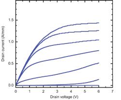 Figure 1: Drain characteristics of 2x(80x50)μm devices for gate voltage ranging from 0V to -6V in steps of -1V.
Direct current (DC) and radio frequency (RF) measurements were carried out. As one might expect, the device operates in a normally-on (depletion) mode. At zero gate voltage (VGS) the maximum drain current is 1.43A/mm. At a gate voltage of -7V and a drain voltage (VDS) of 6V, the current has been pinched-off down to 4.6μA/mm. The device is described as having ‘well-behaved characteristics’, although there is some evidence of short-channel effects with increased output conductance for gate voltages less than -4V and drain voltages greater than 5V (Figure 1).
The peak extrinsic conductance of 415mS/mm is found at a gate voltage of -4.34V and a drain voltage of 4.0V. The gate leakage is 5μA/mm at a gate voltage -8V. The ratio of on- and off-currents is 106 at 4V drain voltage.
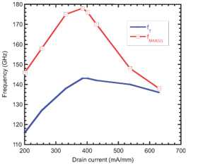
Figure 2: Dependence of fT and fMAX(U) as a function of drain current at 4V drain voltage.
The RF measurements were carried out from DC to 40GHz (Figure 2). Without de-embedding the characteristics of the HEMT from those of the contact pads, the researchers obtained fT and fMAX(U) cutoff frequencies of 100GHz and 144GHz, respectively. Removing the contact pad contributions gave an fT of 143 GHz and an fMAX(U) of 176 GHz.
See related items:
Kopin wins $750,000 SBIR award to develop AlInN HEMT materials
Pushing AlInN and AlGaN HEMTs further on SiC and silicon
![]() Search: AlInN HEMTs AlInN HEMTs
Search: AlInN HEMTs AlInN HEMTs
Visit: http://apex.ipap.jp/link?APEX/3/094101
For more: Latest issue of Semiconductor Today
The author Mike Cooke is a freelance technology journalist who has worked in the semiconductor and advanced technology sectors since 1997.
![]() ©2010 Juno Publishing and Media Solutions Ltd. All rights reserved. Semiconductor Today and the editorial material contained within it and related media is the copyright of Juno Publishing and Media Solutions Ltd. Reproduction in whole or part without permission from Juno Publishing and Media Solutions Ltd is forbidden. In most cases, permission will be granted, if the author, magazine and publisher are acknowledged.
©2010 Juno Publishing and Media Solutions Ltd. All rights reserved. Semiconductor Today and the editorial material contained within it and related media is the copyright of Juno Publishing and Media Solutions Ltd. Reproduction in whole or part without permission from Juno Publishing and Media Solutions Ltd is forbidden. In most cases, permission will be granted, if the author, magazine and publisher are acknowledged.
Disclaimer: Material published within Semiconductor Today and related media does not necessarily reflect the views of the publisher or staff. Juno Publishing and Media Solutions Ltd and its staff accept no responsibility for opinions expressed, editorial errors and damage/injury to property or persons as a result of material published.
Semiconductor Today, Juno Publishing and Media Solutions Ltd, Suite no. 133, 20 Winchcombe Street, Cheltenham, GL52 2LY, UK
Web site by No Name No Slogan ![]()