- News
22 December 2010
Taiwan researchers make steps to improve LED output
Taiwan National Cheng Kung University (NCKU) have used a stepped series of quantum wells to improve electron injection into indium gallium nitride (InGaN) light-emitting diodes (LEDs) by 63% over a comparison conventional LED at 20mA current [Shyh-Jer Huang et al, Appl. Phys. Express, vol3, p122106, 2010]. The improvement over a non-stepped (dual-stage) structure was 20%.
The aim of the research was to improve electron capture rates in multi-quantum well (MQW) LED structures. The researchers relate their work to that carried out by NCKU with charge asymmetric resonance tunneling (CART, 2002) and dual-stage structures (2007) that are used to control the injection of electrons into the MQW light-emitting region. In particular, one wants to avoid overshoot of the electrons over the MQW region, which then recombine in the p-contact region, producing mainly heat and unwanted radiation.
In CART, the ‘electron-emitting layer’ (EL) consists of a thick InGaN region, out of which the electrons are expected to tunnel into the MQW. However, thick InGaN tends to introduce defects into subsequent layers, killing performance.
The new work modifies the dual-stage approach where one has two sets of MQWs – one as an EL and the other as light-emitter/active region. The new variation grades the EL MQW structure from small wells near the n-GaN region to deeper ones next to the active region.
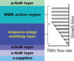 The researchers used metal-organic chemical vapor deposition (MOCVD) to create their epitaxial structure (Figure 1) on c-plane GaN substrates. Trimethyl-metals (TM-) were used for the In and GaN sources; ammonia provided the nitrogen. The magnesium p-doping was provided by bis(cyclopentadienyl) magnesium (Cp2Mg) and the silicon n-doping by disilane (Si2H6).
Figure 1: Stepped electron-emitting layer (EL) LED structure and illustration of flow rate for controlling In composition. EL with six QWs is taken as an example.
A variety of LED structures were produced, including one without an electron-emitting layer (Sample A). Sample B was a dual-stage structure consisting of six 3nm undoped In0.1Ga0.9N quantum wells with 12nm Si-doped GaN barriers. Three further devices were produced with stepped 3nm undoped InxGa1-xN wells and 12nm Si-doped GaN barriers. The indium content of the wells was varied linearly (as determined by In source flow rate). Samples C, D and E had four, six and eight wells, respectively.
The MQW active region of all devices consisted of five In0.21Ga0.79N wells and GaN barriers. The p-contact region consisted of 0.2μm of GaN. The structures were converted into devices using standard LED processes.
Before this, the structures were analyzed using high-resolution x-ray diffraction (HR-XRD) and photoluminescence (PL) from excitation by 325nm light from a helium–cadmium laser. The x-ray analysis suggests that the dual-stage and graded EL regions also act as strain relaxer/buffer, resulting in better material quality in the subsequent MQW active layers. The greater photoluminescence with EL layers over structures without EL layers supports this analysis.
In terms of electrical performance, the I–V curves show a reduced forward voltage for the EL devices. It is believed from this that a further benefit of the EL layer is to give a better spreading of current in the LEDs.
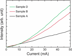 At low currents (<10mA), the light outputs are similar. However, as the current increases the curves separate (Figure 2). The stepped structure gives the highest light output. At 20mA, the stepped LED has 63% and 20% increase in light output over the conventional and dual-stage devices, respectively.
Figure 2: Light output vs current characteristics for conventional, dual-stage and stepped LEDs (samples A, B, and D, respectively).
In terms of the number of steps, the six-stage (Sample D) device is a significant improvement over the four-stage component (Sample C). However, going to eight stages offers only a minimal bump in light output.
The research was carried out with money from the university, ‘‘Lamp Development of White Light-Emitting Diode for Local Lighting’’ TDPA (Technology Development Program for Academia), and Taiwan’s National Science Council.
Virginia Commonwealth University (VCU) has also recently been using a modified scheme to inject electrons into LED active regions. The aim of the VCU approach was also to reduce the electron overspill into the p-GaN layer by cooling the electron distribution with a staircase injector. An MQW underlayer was employed to maintain material quality.
Unveiling hot-electron over-spill in nitride LEDs
MQW LEDs GaN MOCVD
The author Mike Cooke is a freelance technology journalist who has worked in the semiconductor and advanced technology sectors since 1997.