- News
8 December 2010
UCSB uses more uniform InGaN for record efficiency semi-polar green LED
Researchers at University of California Santa Barbara (UCSB) have produced semi-polar green light-emitting diodes (LEDs) with external quantum efficiencies of 20.4% [Shuichiro Yamamoto et al, Appl. Phys. Express, vol3, p122102, 2010]. The team also included one researcher each from Sharp Corp and Mitsubishi Chemical Corp.
The UCSB group produced both green and green-yellow LEDs using gallium nitride (GaN) crystal substrates oriented in the (20-21) direction.
The electroluminescence of the green LED at 20mA had an output power of 9.9mW and external quantum efficiency (EQE) of 20.4% under pulsed operation (10% duty cycle). This changed only slightly by moving to DC operation, with 9.2mW output power and 19.1% EQE.
The researchers comment: ‘To the best of our knowledge, these output powers and EQEs at a driving current of 20mA are the highest values that have ever been reported for green LEDs grown on semi-polar/non-polar planes.’
The yellow-green LEDs had 5.7mW output power and 12.6% EQE under a pulsed current of 20mA. The DC figures were 5.2mW and 11.6%, respectively.
The researchers conclude: ‘These results suggest that (20-21) GaN substrates could be one of the possible substrates for high-power and high-efficiency LEDs with green or even longer wavelengths.’
Researchers have been expending much effort to improve green nitride LED efficiency. For the most mature devices grown in the c-direction of the nitride crystal structure, an EQE of 30% was reached in 2007.
However, for these devices there are known effects that hamper further progress. The most prominent of these is the quantum-confined Stark effect (QCSE), where polarization electric fields due mainly to strain effects (piezoelectricity) tend to pull apart the electrons and holes that are desired to recombine into photons, reducing efficiency.
The QCSE gets worse as the desired wavelength of the device gets longer because one is trying to combine light-emitting layers of higher-indium-content indium gallium nitride (InGaN) with a gallium nitride (GaN) substrate lattice parameter. This creates a large strain in the InGaN and hence a large piezoelectric polarization electric field.
The past few years have seen a number of research groups exploring different growth directions in nitride semiconductors with reduced (semi-polar) or even zero (non-polar) polarization. These efforts have not as yet reached the efficiency of c-plane devices, partly due to the immaturity of knowledge of how to grow high-quality material, partly due to new intrinsic difficulties.
The substrates for the new UCSB (20-21) LEDs were prepared by slicing a c-plane GaN bulk crystal in the appropriate direction. The bulk crystal was grown using hydride vapor phase epitaxy (HVPE).
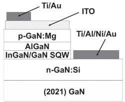 Figure 1: Schematic of UCSB’s green and yellow-green LED device structures on (20-21) substrate.
The LED semiconductor layers (Figure 1) were grown using metal-organic chemical vapor deposition (MOCVD). The active region consisted of a single quantum well (SQW) of 3.5nm-thick InGaN sandwiched between GaN barriers. An electron-blocking layer (EBL) consisting of magnesium-doped AlGaN was used to keep the electrons in the well region, and thus to increase recombination as photons, rather than in the p-type Mg-doped GaN contact.
A 250nm tin-oxide-doped indium oxide layer (ITO) was applied by electron-beam deposition and annealing to make a p-type transparent contact. Metal contacts were then applied, first to the n-GaN layer and then to the p-GaN layer.
The backside of the GaN substrate was roughened to increase light extraction from the device. The diced LEDs were mounted on transparent zinc oxide material as a submount and then packaged in silicone resin in a ‘vertical stand’ configuration.
The emission peak wavelength of the green device was 516.3nm at 20mA. The peak wavelengths at 1mA and 80mA were 529.9nm and 511.9nm, respectively. The shortening of the wavelength with current (‘blue-shift’) is attributed mainly to the effect of the applied bias on the QCSE.
An alternative explanation would be band-filling effects caused by potential fluctuations due to the inhomogeneity of the InGaN material. Band-filling is used to explain a marked narrowing of the emission line spectrum in green LEDs grown on (11-22) substrates in the low current range. However, this behavior was not seen in the (20-21) green LEDs and the linewidths were about the same across the current range. The researchers believe that by growing on the (20-21) plane they have ‘substantially improved’ the uniformity of the InGaN QW.
The blue-shift observed of 4.4nm between 20mA and 80mA was also smaller than that seen in (11-22) devices, where a value of 12.4nm between 20mA and 100mA was previously reported.
For the yellow-green devices, peak wavelengths were 572.5nm, 552.3nm, and 544.2nm at 1mA, 20mA, and 80mA, respectively. The 20mA to 80mA blue-shift of 8.1nm is larger than for the green device, but still smaller than that of the (11-22) green device.
Line-width narrowing is also not observed in the yellow-green LEDs. At 10mA, the line-widths for the green and green-yellow (20-21) devices were 33.0nm and 40.8nm, respectively. The published (11-22) green device had a 42.5nm linewidth. The narrower line-widths of the (20-21) devices are again taken as indication that the InGaN layer had better uniformity and hence fewer potential fluctuations.
The operating voltages are rather high – i.e. 6.4V (green) and 6.8V (green-yellow) – indicating that the upper layers (p-GaN and ITO) need optimizing.
UCSB achieves semi-polar light extraction comparable to conventional LEDs
Semi-polar green LEDs GaN InGaN AlGaN MOCVD
The author Mike Cooke is a freelance technology journalist who has worked in the semiconductor and advanced technology sectors since 1997.