| Home | About Us | Contribute | Bookstore | Advertising | Subscribe for Free NOW! |
| News Archive | Features | Events | Recruitment | Directory |
News
24 February 2010
Seeking ultra-low ohmic path to high-frequency nitride transistors
A ‘very low ohmic contact’ of 0.1Ω-mm has been made to nitride semiconductor high-electron-mobility transistor (HEMT) structures produced at University of California Santa Barbara [Nidhi et al, Jpn. J. Appl. Phys., vol49, p021005, 2010]. The researchers comment: “Ultralow ohmic contact resistance of 0.1Ω-mm was achieved, which is among the lowest reported values for alloyed contacts to GaN HEMTs.”
Nitride HEMTs are attractive for high-frequency power amplification and power switching applications. Low levels of parasitic components such as contact resistances are particularly vital for high-frequency devices and for reducing power consumption. The UCSB work is aimed at enabling sub-micron high-frequency transistors with recessed gates.
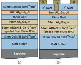 Figure 1: Schematic of UCSB epitaxial layer structure (left) and standard HEMT with recessed gate (right).
The low-resistance contacts were produced by using the nitrogen-face of the top gallium nitride (GaN) layer in a HEMT device structure (Figure 1). Devices more frequently use the gallium-polar orientation of the GaN crystal structure (0001) since it is easier to grow as high-quality layers. However, attracted by the lower contact resistance of N-polar material (000-1), advances have recently been made in its growth using molecular beam epitaxy (MBE) and metal-organic chemical vapor deposition (MOCVD).
The UCSB structure was grown using MOCVD on (0001) sapphire (4° miscut toward a-plane) with ammonia, trimethyl-gallium and trimethyl-aluminum sources for N, Ga and Al. Silicon was used for n-type doping and iron for creating a semi-insulating buffer with sources disilane and bis(cyclopentadienyl)-iron, respectively.
The channel consisted of a 15nm layer of GaN on top of aluminum gallium nitride (30% Al), creating a two-dimensional electron gas towards the interface. The ohmic contacts were formed by electron-beam evaporation of Ti/Al/Ni/Au. The purpose of the upper AlGaN layer is to serve as an etch stop. Previously, AlGaN has been used as a stop layer for Ga-face GaN etching.
Initial measurements of the UCSB structure, with surface ‘ohmic’ contacts, demonstrated Schottky-type behavior, “most likely caused by the formation of a polarization-induced Schottky barrier (ΦB) in the AlGaN due to sign of the polarization”.
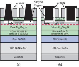
Figure 2: Angled evaporation of contact metals enables better sidewall alloy contact and hence creates a wider current path to channel (left 0°, right 40°).
To overcome this problem, the contact regions were etched with boron trichloride/chlorine plasma, removing the top GaN and AlGaN layers. Evaporation was carried out at different angles to increase the side-wall coverage with contact metal (Figure 2). Angled evaporation overcomes mask shadowing effects. The wafer was rotated during evaporation for even coverage. Alloying was carried out at 870°C.
Transfer length measurements (TLM) were made to determine the respective contact resistances, which decreased from 0.5Ω-mm for 0° evaporation angle down to almost 0.1Ω-mm at 40°. TLM (also known as transmission line measurement) is used to measure contact resistance by plotting resistance values measured between pads separated by varying lengths versus the spacing. The vertical intercept gives the contact resistance (ohm-mm), the slope gives the sheet resistance and the horizontal intercept gives the transfer length.
Since writing the paper, one of the researchers, Nidhi, reports that her group (led by professor Umesh K Mishra) has used these ‘funnel contacts’ in transistors with a deep-recess gate structure, and that the data has been submitted to the International Symposium on Compound Semiconductors (ISCS, Japan, 31 May–4 June 2010). Work on funnel contacts has also been carried out with silicon carbide substrates, where similar results were found.
See related items:
Gate control of terahertz transistor emission frequency
Reducing GaN HEMT degradation with InAlN barrier
![]() Search: GaN HEMT AlGaN MOCVD MBE
Search: GaN HEMT AlGaN MOCVD MBE
Visit: http://jjap.ipap.jp/link?JJAP/49/021005
Visit: http://my.ece.ucsb.edu/mishra/research.htm
The author Mike Cooke is a freelance technology journalist who has worked in the semiconductor and advanced technology sectors since 1997.
![]() ©2010 Juno Publishing and Media Solutions Ltd. All rights reserved. Semiconductor Today and the editorial material contained within it and related media is the copyright of Juno Publishing and Media Solutions Ltd. Reproduction in whole or part without permission from Juno Publishing and Media Solutions Ltd is forbidden. In most cases, permission will be granted, if the author, magazine and publisher are acknowledged.
©2010 Juno Publishing and Media Solutions Ltd. All rights reserved. Semiconductor Today and the editorial material contained within it and related media is the copyright of Juno Publishing and Media Solutions Ltd. Reproduction in whole or part without permission from Juno Publishing and Media Solutions Ltd is forbidden. In most cases, permission will be granted, if the author, magazine and publisher are acknowledged.
Disclaimer: Material published within Semiconductor Today and related media does not necessarily reflect the views of the publisher or staff. Juno Publishing and Media Solutions Ltd and its staff accept no responsibility for opinions expressed, editorial errors and damage/injury to property or persons as a result of material published.
Semiconductor Today, Juno Publishing and Media Solutions Ltd, Suite no. 133, 20 Winchcombe Street, Cheltenham, GL52 2LY, UK
Web site by No Name No Slogan ![]()