| Home | About Us | Contribute | Bookstore | Advertising | Subscribe for Free NOW! |
| News Archive | Features | Events | Recruitment | Directory |
News
8 March 2010
Jenoptik opens laser application center in Korea
After starting construction last July and moving in last November, Germany’s Jenoptik Group has formally opened its new sales, application and service site in the southern Korean city of Pyeongtaek (Gyeonggi province, 70km south of Seoul) in the presence of about 100 invited guests from business and politics as well as customers and partners in Asia.
The new center is part of the expansion of Jenoptik Korea Corp Ltd, which was founded last July as a partnership between Jenoptik AG (66.6%) and Telstar-Hommel Corp (33.3%), a long-standing Jenoptik joint venture partner in the Industrial Metrology division. “Without the close and intensive collaboration, we would not have been able to build the laser application center so quickly,” said Jenoptik Group’s chairman of the executive board Dr Michael Mertin and chief financial officer Frank Einhellinger in thanking Telstar-Hommel’s president & CEO Buyng-Hoon Im.
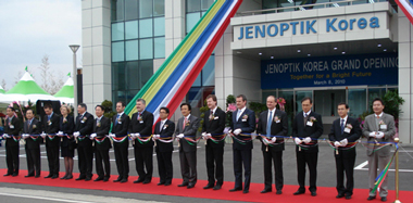
Picture: Jenoptik opens its new sales, application and service site in the southern Korean city of Pyeongtaek.
A total of over 60 Jenoptik laser systems for various applications are currently in use in Asia, and 14 further systems have been commissioned and will be delivered or installed in the coming months. The firm says that Jenoptik Korea Corp Ltd achieved its first successes more quickly than expected and has received new orders worth about €5m in recent months.
Covering 500m2 (including 80m2 of cleanroom) on a campus shared with Telstar-Hommel and costing $4.4m (€3.4m/Won 5.4bn), the new laser application center has initially been equipped with two laser systems for processes in the electronic as well as photovoltaics and flat-panel industries. The Jenoptik VOTAN Semi 300 is designed for machining wafers (Si, GaAs or SiC) and thus also for ultra-precise applications in cleanroom environments. The special separation process developed by Jenoptik — TLS-Dicing (where TLS = Thermal Laser Separation) — enables quick, efficient and damage-free separation of semiconductor wafers, says the firm. With the Jenoptik VOTAN Advanced laser system, the TLS process specifically addresses the photovoltaics and flat-panel industry for separating thin-film solar cells and display glass.
Customers and interested parties from across Asia in the areas of electronic, flat panel as well as photovoltaics and automotive can now test lasers and laser applications for their own production environments on site with their own materials. In addition to tests, together with Jenoptik engineers they can also develop individual processes on the systems, manufacture pilot runs and small batches, and commission feasibility studies. Also, in the coming months, Jenoptik plans to expand the application center with additional laser systems.
With eight staff, Jenoptik Korea Corp Ltd is also in charge of all after-sales service in Asia together with other Jenoptik firms, e.g. in Japan. The Jenoptik Group currently has a total of about 150 staff in its own or in joint venture firms in Asia since, in addition to Korea, it is also present in China and Japan.
“This moves our process of internationalization a major step forward,” said Mertin of the new center. “Direct market access and a trained service team are indispensable for complex systems,” he added. “With the new center, we have laid the foundation for further business activities of all divisions of the Jenoptik Group.”
According to preliminary figures, sales of the Jenoptik Group in Asia comprised just under 8% of the group’s overall sales of about €470m in 2009; just under 10% of overall sales in the Lasers & Optical Systems segment were in Asia. “We see more great potential for the overall group in Asia,” said Mertin. “With our direct local presence, we can now approach the market better and more intensively.”
See related item:
Jenoptik showcases TESAG epiwafer acquisition
![]() Search: Jenoptik GaAs wafers SiC wafers Lasers
Search: Jenoptik GaAs wafers SiC wafers Lasers
Visit: www.jenoptik.com
![]() ©2010 Juno Publishing and Media Solutions Ltd. All rights reserved. Semiconductor Today and the editorial material contained within it and related media is the copyright of Juno Publishing and Media Solutions Ltd. Reproduction in whole or part without permission from Juno Publishing and Media Solutions Ltd is forbidden. In most cases, permission will be granted, if the author, magazine and publisher are acknowledged.
©2010 Juno Publishing and Media Solutions Ltd. All rights reserved. Semiconductor Today and the editorial material contained within it and related media is the copyright of Juno Publishing and Media Solutions Ltd. Reproduction in whole or part without permission from Juno Publishing and Media Solutions Ltd is forbidden. In most cases, permission will be granted, if the author, magazine and publisher are acknowledged.
Disclaimer: Material published within Semiconductor Today and related media does not necessarily reflect the views of the publisher or staff. Juno Publishing and Media Solutions Ltd and its staff accept no responsibility for opinions expressed, editorial errors and damage/injury to property or persons as a result of material published.
Semiconductor Today, Juno Publishing and Media Solutions Ltd, Suite no. 133, 20 Winchcombe Street, Cheltenham, GL52 2LY, UK
Web site by No Name No Slogan ![]()