- News
24 November 2010
Ohio boosts nitride tunneling current to 118A/cm2 at –1V
Researchers at Ohio State University have achieved ‘the highest current density reported for III-nitride tunnel diodes' [Sriram Krishnamoorthy et al, Appl. Phys. Lett., vol97, p203502, 2010]. The work employed the narrower-bandgap material indium gallium nitride (InGaN) for the tunneling barrier rather than the usual wider-bandgap aluminum gallium nitride (AlGaN). At –1V, the current density of the new device was 118A/cm2. The maximum current density was 9.2kA/cm2 (limited by the capability of the measuring equipment).
Tunnel junctions can be used to create low-resistance connections between devices such as light-emitting diodes (LEDs), laser diodes, multi-junction solar cells, and tunnel field-effect transistors (TFETs).
In wide-bandgap nitride light-emitting devices, there are problems in creating low-resistance p-contacts especially, and here tunnel junctions could be useful in allowing n-type material to contact with the hole injection layer.
For example, Korean researchers from Lumimicro Co Ltd, Kyungpook National University, Korea Photonics Technology Institute, and Pukyong National University recently used a LED epiwafer from Epivalley with a three-period InGaN (In 17%) tunnel junction structure to give an n-type zinc oxide transparent conducting layer a suitable contact with the underlying p-GaN layer (Al-Ga co-doped ZnO conducting layer boosts nitride tunnel junction LED). Unfortunately, the external quantum efficiency was quite low (~23%) compared with some leading commercial devices (~60%).
 The Ohio team designed its tunnel junction structure (Figure 1) by using simulations and semi-classical (Wentzel–Kramers–Brillouin = WKB) theory to understand how to use polarization electric fields (spontaneous and piezoelectric/strain-dependent) and band-bending effects to increase the tunneling probability and hence the current. These studies suggested that there was a critical thickness for the barrier. Below this, the conduction band on one side is not aligned suitably with the valence band on the other. Above the critical value, the tunneling probability is reduced by the thickness of the barrier.
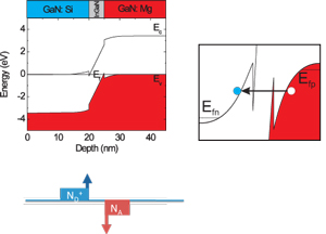
Figure 1: Left: schematic and equilibrium energy band diagram of GaN/InGaN/GaN (In 33%) zero-bias interband tunnel junction. Right: band diagram at reverse bias, showing interband tunneling.
The critical thickness is reduced (and hence the expected current increased) as the In molar fraction of the InGaN barrier is increased. However, it can be difficult to create high-quality InGaN with high In concentrations.
InGaN tunnel junctions were grown on an N-polar free-standing GaN substrate, using plasma-assisted molecular beam epitaxy (PAMBE). The growth system used was Veeco’s Gen 930 tool. Lumilog supplied the LED-quality GaN template. The researchers used N-polar material because higher indium concentrations have been achieved with such material.
The n-type GaN layer was grown first with a heavy (n+) silicon-doping donor density of 5x10¹⁸/cm3 and 100nm thickness. This was followed by the InGaN layer, which was measured using x-ray diffraction to be 6.4nm thick with a 33.5% indium composition. The final p-type GaN layer was also 100nm and had a heavy (p+) magnesium acceptor density of 1x10¹⁹/cm3.
Reference p–n junctions, without the InGaN tunnel layer, were also grown. The metals used for the p-contact were nickel-gold, and for the n-contact, titanium-gold.
The tunnel junction (TJ) had higher current flow in both directions compared with the p-n junction (Figure 2). The reverse current of the tunnel junction was several orders of magnitude higher than that of the p–n reference.
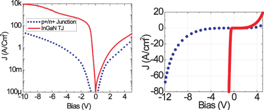
Figure 2: Left: log J–V characteristics of GaN/InGaN/GaN TJ (solid line) and standard p+/n+ junction (dotted). Right: same characteristics plotted using linear J-axis.
The p–n junction shows the standard behavior, where the reverse bias current is lower than that under forward bias. The tunnel junction, by contrast (but as expected for such ‘backward-diode’ devices), has a higher current under reverse-bias compared with the forward condition.
The tunnel junction device has a steep turn-on region of 70–130mV/decade close to zero-bias for tunneling. The researchers comment: “Such a low turn-on voltage would be an ideal candidate to connect devices in series, especially in the case of multiple active-region emitters”.
At 1V reverse bias, the current density is 118A/cm2 (the p–n current was five orders of magnitude lower). At higher reverse bias values the differential resistance increases significantly. The researchers suggest that increased series and contact resistance, along with self-heating effects, may be to blame, although ‘further analysis is needed to understand the origin of this behavior.
Despite this, the researchers measured a maximum current density of 9.2kA/cm2 (limited by the capability of the measuring equipment). This value is claimed to be ‘the highest current density reported for III-nitride tunnel diodes’.
The researchers plan to improve the structure with higher indium compositions and optimized barrier thicknesses. The team is also looking into ‘further sophistication with graded GaN/InGaN interfaces, asymmetric junctions, and quaternary alloys, with a view to lower resistance and higher tunneling current. Improved understanding of the theory and modeling will also be pursued.
It is also suggested that other material systems might benefit from using narrower-bandgap tunneling materials such as AlGaN, AlN and ZnO.
The researchers conclude: ‘The tunnel junction designs demonstrated here will enable the incorporation of tunnel junctions in several technologically relevant III-nitride devices such as LEDs, lasers, and solar cells, and provide a pathway to device structures such as tunnel FETs.’
Some of the funding for the research came from the US Office of Naval Research (ONR).
The author Mike Cooke is a freelance technology journalist who has worked in the semiconductor and advanced technology sectors since 1997.