- News
22 November 2010
SEI’s {20-21} semi-polar green laser lowers threshold current by 2–3x
Japan’s Sumitomo Electric Industries (SEI) has presented detailed performance measurements of a series of green lasers diodes (LDs) based on its semi-polar {20-21} free-standing gallium nitride (GaN) substrates [Masahiro Adachi et al, Appl. Phys. Express, vol3, p121001, 2010].
A number of companies and other research groups are racing to develop stable and efficient green laser diodes with a view to replacing bulky full-color projector systems that use an infrared diode to excite a second-harmonic generator material that creates green light. Single laser diode solutions are already used to create blue and red light. These are based on indium gallium nitride (InGaN) and aluminum gallium indium phosphide (AlGaInP) technologies, respectively.
The advantages of using a single lasers diode based on nitride semiconductor technology are expected to be compactness and stability. Nitrides are presently preferred for this over II-VI semiconductor alternatives since they are expected to eventually have longer, practical lifetimes.
SEI produced the first true green nitride lasers diodes last year, with devices having emission wavelengths up to 531nm. Since then, other groups have achieved green lasing on traditional c-plane GaN. However, semi-polar devices are expected to perform better in many respects due to a reduced polarization electric field in the active layers.
Nitride semiconductors have both spontaneous and piezoelectric (strain-dependent) polarization. Differences in these properties between different layers of material give rise to effective surface charges and hence electric fields in addition to those applied externally. These fields tend to pull the electron and hole carriers apart in the active region, making recombination into photons (and hence laser light) more difficult. This quantum-confined Stark effect (QCSE) hence raises the threshold current for lasing. Hence, researchers are keen to reduce threshold currents and voltages, with a view to lower operating voltages and higher wall-plug efficiency.
The polarization fields are strongest in the c-plane direction. By growing nitride semiconductors in other crystal directions, the QCSE can be reduced. The lower density of states for holes and higher transition matrix elements for optical gain due to valence-band splitting are also seen as advantages of semi-polar structures. Experiment has also shown the quality of InGaN layers to be more homogeneous on {20-21} material, compared with c-plane grown films.
SEI uses hydride vapor phase epitaxy (HVPE) to produce its {20-21} substrates. The company has managed to reduce threading dislocation densities to less than 10-6/cm2. The material is n-type conductive and the resistivity (0.01Ω-cm) is such that back-contacts can be used for vertical current flow through the device (unlike with lasers diodes on insulating sapphire or more resistive GaN).
The epitaxial lasers diode layers with separate-confinement heterostructures (SCHs) were deposited using metal-organic chemical vapor deposition (MOCVD). Gain-guided (10μm waveguide width) and ridge-waveguide (2μm) lasers diodes were produced. The 600μm-long cavities were produced along the advantageous [-1014] direction. Appropriate dielectric mirrors were used to minimize losses.
Testing for thresholds was carried out using pulsed operation (0.5μsec pulse, duty cycle 0.5%) at room temperature for the gain-guided lasers diodes. Pulsed testing is often used to avoid self-heating effects. The ridge device were subjected to continuous wave (cw) operation.
The threshold current in the 520–530nm green range was nearly half that of traditional c-plane devices (Figure 1). The current density threshold varied between 3.4kA/cm2 at 511nm and 5.4kA/cm2 at the longest wavelength of 533.6nm. The researchers credit optimized quantum well structures and growth conditions for these achievements.
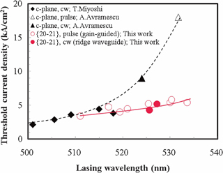 Figure 1: Dependence of threshold current density on lasing wavelengths. Open and solid circles: gain-guided and ridge-waveguide green LDs on {20-21} semi-polar planes, respectively. Triangle and diamond: LDs on c-plane published by Nichia and Osram Opto Semiconductors. Solid and open symbols, including triangles and circles: cw and pulsed operation, respectively. Solid and broken lines are trend guides for the eye.
These results run in the face of theoretical expectations that {20-21} lasers diodes will have threshold current of 65% that of the equivalent c-plane device. In the long-wavelength region (>520nm) the semi-polar device is much better (2–3x lower) than the c-plane devices, and in the short-wavelength region it tends to be about the same as the c-plane device.
The researchers comment: “The reason for the disagreement may be due to the differences in the crystal quality between the semi-polar {20-21} and the c-plane lasers diodes, i.e. the difference in the compositional homogeneities of the InGaN quantum wells, which is not considered in the theoretical studies”.
They add: “We believe the experimental results in this work indicate that the deterioration of the crystal quality of the InGaN active layers over 520nm is much less severe for the {20-21} plane compared to the c-plane”.
The team also reports in more detail on ‘a typical ridge-waveguide green LD in cw operation at RT lasing at the wavelength of 525.5nm’. The threshold current, current density and voltage were 51.1mA, 4.3kA/cm2, and 6.38V, respectively. The slope efficiency was 0.15W/A. With the mirrors used, the output power was 36.4mW under cw operation at 25°C.
The researchers plan further optimizations for high-power operation, with a report due in the ‘near future’.
The T0 characteristic of the 525nm lasers diode threshold current temperature variation (proportional to exp(T/T0)) of 175K was measured using temperature control and pulsed operation. This compares with lower values for c-plane devices of 145K at 518nm and 120K at 515nm measured by the Nichia group. A higher T0 indicates smaller variation of the threshold with absolute temperature.
Far-field pattern divergence was also measured at 2mW output and 25°C: the perpendicular and parallel divergence angles at half power were 24° and 11°, respectively. These are slightly larger than the corresponding measurements for Nichia’s c-plane devices: 22.8° and 10.4°, respectively.
“This indicates that the symmetry and optical confinement of the {20-21} green LD with InAlGaN cladding layer are comparable to the conventional c-plane InGaN LDs,” says the researchers.
Green laser diode market $500m by 2016 as pico-projector market drives growth
SEI explains polarization clues to optimal GaN green laser stripes
SEI Green lasers Free-standing GaN substrates HVPE MOCVD
The author Mike Cooke is a freelance technology journalist who has worked in the semiconductor and advanced technology sectors since 1997.