- News
31 August 2011
Passivated AlInN/GaN HEMT pushes beyond 200GHz cut-offs
Researchers in Switzerland report the first realization of fully passivated aluminum indium nitride on gallium nitride (AlInN/GaN) high-electron-mobility transistors (HEMTs) with cut-off frequencies in excess of 205GHz [Stefano Tirelli et al, IEEE Electron Device Letters, published online 15 August 2011]. The work was based at ETH Zürich’s Millimeter-Wave Electronics Group and the Institute of Quantum Electronics and Photonics of École polytechnique fédérale de Lausanne (EPFL).
AlInN growth has been developed and improved as a promising barrier component in HEMT structures, allowing smaller devices compared with aluminum gallium nitride (AlGaN) barriers. AlInN allows higher electron densities to form at the barrier/buffer interface and has less surface depletion effects than AlGaN. This allows thinner barrier layers to be used, so that the need for recess etching to bring the gate contact closer to the channel region of the device is avoided. Etching can damage device performance and reliability.
Early work on AlInN/GaN HEMTs has tended to use unpassivated devices to show the possibility of the technology, since passivation increases parasitic capacitance effects. However, for long-term reliability and control of surface states, passivation layers are needed.
RF measurements were carried out up to 40GHz. De-embedding of the effect of the contacts was carried out to give cut-off (fT) and maximum oscillation (fMAX) frequencies of 205GHz and 220GHz, respectively, at drain and gate biases of 5V and –5.4V, respectively. Increasing the drain bias to 6V allowed an even higher fMAX of 230GHz with a gate potential of –5.6V. Around gate potentials of –5.5V, fT and fMAX remain above 200GHz (Figure 1) for a broad range of drain bias conditions (2.5–10V).
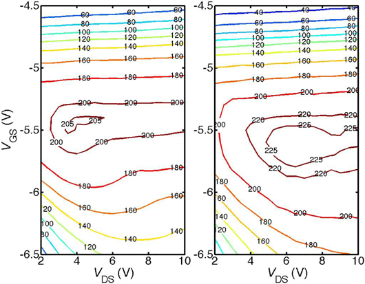
Figure 1: Drain (VDS and gate (VGS) bias dependence of fT (left) and fMAX (right). The values are shown in gigahertz on the contour maps.
Previous work with 100nm-gate-length passivated AlInN/GaN HEMTs had fT/fMAX values of 144/137GHz. The researchers comment that, even with a thin passivation, LG must nearly be halved compared to the 55nm unpassivated devices in their previous work to maintain fT above 200GHz in a passivated HEMT.
MIT/Notre Dame recently produced unpassivated devices with 30nm gate that had fT/fMAX values of 245/13GHz.
Comparing their small-signal model with that of a device with low-resistance re-grown ohmic contacts resulting in fT/fMAX of 220/289GHz produced by HRL Laboratories in the USA, the Swiss researchers believe that their device’s fT performance is limited by the relatively large gate–channel distance, resulting in restricted transconductance.
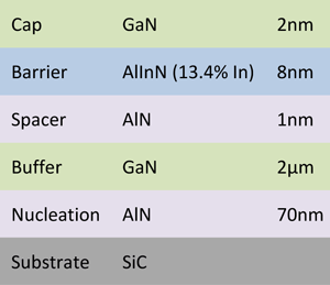 The HEMT epitaxial layers (Figure 2) were grown at EPFL on semi-insulating silicon carbide. The gate-to-channel distance was 11nm (1+8+2nm). The GaN cap was added to reduce gate leakage currents.
Figure 2: Schematic of epitaxial layers used for HEMT.
The ohmic source–drain contacts consisted of evaporated titanium-aluminum-molybdenum-gold, rapidly thermal annealed at 860°C. The contact resistance was measured at 0.3Ω-mm with a channel sheet resistance of 180Ω/square. The device regions were isolated using a phosphorus/helium ion implant.
T-shaped gates were formed using a three-layer electron-beam lithography process. The gate was 100μm wide with two fingers extending from a central contact (2x50μm). The gate was placed in the middle of the 1μm source–drain gap. The T-head of the gate was 400nm, while the base was 30nm. In fact, the actual cross-section of the gate was more Y-shaped (Figure 3). The metal structure of the gate was nickel-platinum-gold, giving a Schottky junction with the underlying semiconductor.
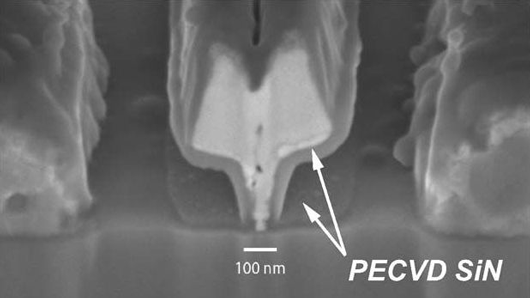
Figure 3: Micrograph of reported device after a focused-ion beam (FIB) cut. Partial removal of SiN in proximity of the ohmic contacts is an artifact of the FIB preparation process. HEMTs were fully covered for the measurements.
The device was then passivated with a 60nm layer of silicon nitride, deposited using plasma-enhanced chemical vapor deposition (300°C). The contacts were accessed using a sulfur hexafluoride plasma etch. The overlay wiring and measurement pads consisted of titanium-copper-gold.
DC measurements gave an extrinsic transconductance peak of 462mS/mm at drain bias 1V. The gate leakage with the gate at –7V was 4.4μA/mm at 0V drain, rising to 10μA/mm at 10V drain. These performance figures are comparable to those recently achieved by the group without passivation or GaN cap layer. The on-resistance was 1.1Ω-mm, with more than two-thirds of this coming from the contacts. The maximum drain current at 0V gate potential was 2.18A/mm.
Channel pinch-off is not achieved with higher drain bias. This is attributed to drain-induced barrier lowering associated with the gate-length/gate-channel-distance ratio of 2.7 (= 30/11). Pulse current–voltage (500ns) measurements at gate potentials of 0V and –6V show less than 30% current reduction. The ‘quiescent’ period corresponds to gate and drain potentials of –8V and 8V, respectively. The researchers comment: “Collapse is moderate, considering that the 30nm-gate devices are stressed with 16V of quiescent reverse GD bias.”
Nitride HEMT on silicon achieves 143GHz current gain cut-off frequency
Pushing AlInN and AlGaN HEMTs further on SiC and silicon
The author Mike Cooke is a freelance technology journalist who has worked in the semiconductor and advanced technology sectors since 1997.