- News
22 February 2011
EVG adds EVG620HBL mask aligner for HB-LEDs, boosting throughput and yield
At this week’s Strategies in Light 2011 event in Santa Clara, CA, USA (22–24 February), EV Group (EVG) of St Florian, Austria, which makes wafer-bonding and lithography equipment for the advanced semiconductor and packaging, MEMS, silicon-on-insulator (SOI) and emerging nanotechnology markets, is launching the latest addition to its portfolio of products created to optimize manufacturing of high-brightness light-emitting diodes (HB-LEDs), compound semiconductors and power electronics.
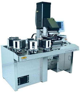 The EVG620HBL fully automated mask alignment system builds on EVG’s field-proven mask aligner platform, adding a high-intensity ultraviolet (UV) light source and five cassette stations — significantly more than competitive offerings, it is claimed — to enable continuous fabrication of devices. The EVG620HBL hence delivers throughput of up to 165 six-inch wafers per hour (up to 220 wafers per hour in first print mode) with what is claimed to be the industry’s highest alignment accuracy and yield.
Picture: EV Group's EVG620HBL fully automated mask alignment system.
According to market research firm Global Information Inc, the consumption of HB-LEDs will continue to grow at rapidly over the next decade, from $10.09bn in 2010 to $46.05bn in 2020. Key drivers will include explosive growth in solid-state lighting and general lighting applications, as well as signage, professional displays, and stationary (non-vehicle) signals. To meet this increased demand, HB-LED makers must quickly ramp up to higher production capacity, as well as optimizing their manufacturing processes to ensure the highest yields — all of which elevates their need for automated manufacturing solutions with the lowest cost of ownership, says EVG.
As with its dedicated EVG560HBL automated wafer-bonding system introduced last July, EVG developed the EVG620HBL aligner to address these needs. The firm notes that its bonders and mask aligners are being deployed by four of the top five major HB-LED makers. Building on this, the 620HBL was created in response to demand for a mask alignment system dedicated to meeting these devices’ yield and throughput requirements.
Another feature of the EVG620HBL is the availability of special recipe-controlled microscopes whose illumination spectrum is optimized to ensure the best pattern contrast with various wafer and layer materials, including substrate materials such as sapphire, silicon carbide (SiC), aluminum nitride (AlN), metal and ceramic. The new mask aligner also features high-accuracy handling and alignment of fragile or warped wafers.
“Just last month, one of the leading HB-LED manufacturers ordered an EVG560HBL bonder, and the EVG620HBL is the latest result of our ongoing efforts around enabling HB-LED manufacturers to develop more efficient, cost-effective and higher-yielding devices to meet their customers' demands,” says executive technology director Paul Lindner.
Join Semiconductor Today's LinkedIn networking and discussion group