- News
29 January 2011
Normally-off nitride semiconductor tunnel junction FET with high drive
Hong Kong University of Science and Technology (HKUST) researchers have produced normally-off nitride semiconductor field-effect transistors with a drive current of 326mA/mm and an on–off ratio of 1010 [Li Yuan et al, ‘Normally Off AlGaN/GaN Metal–2DEG Tunnel-Junction Field-Effect Transistors’, IEEE Electron Device Letters, published online 6 January 2011].
Attempts to use tunnel junctions to improve silicon metal-oxide-semiconductor FET (MOSFET) performance have usually suffered from low drive currents. Similar problems have been seen in GaN MOSFETs (drive current less than 5mA/mm).
The HKUST researchers have taken advantage of the particular conditions in nitride semiconductor high-electron-mobility transistor (HEMT) epitaxial structures with a two-dimensional electron gas (2DEG) to produce their tunnel junction field-effect transistor (TJ-FET).
The thin 2DEG forms at gallium nitride/aluminum gallium nitride (GaN/AlGaN) interfaces due to strong spontaneous and piezoelectric (strain-dependent) polarization electric fields. When a Schottky source metal is used the barrier height (SBH) is of the order of 0.8eV, while the width (SBW) is only a few nanometers. These features create the conditions for efficient quantum tunneling with larger currents.
An added attraction of the HKUST approach is the normally-off, positive threshold behavior. Such devices are sought to reduce power consumption in applications. Conventional nitride semiconductor HEMTs are normally-on, although a number of research groups have demonstrated normally-off behavior using different techniques.
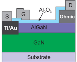 The HKUST researchers developed their device using the epitaxial structure for a standard nitride semiconductor HEMT on Si (111) substrate (Figure 1). The undoped GaN buffer layer was 1.8μm thick and the AlGaN barrier 18nm. The barrier was completed with a 2nm GaN cap layer. A 1nm AlN interface enhancement layer was used between the AlGaN barrier and the GaN buffer for the purpose of reducing alloy scattering of the 2DEG.
Figure 1: Schematic cross section of an AlGaN/GaN TJ-FET.
The main differences from a normal HEMT is in the metallization — in particular, the use of a Schottky source electrode and a tunnel junction gate. The device fabrication began with reactive ion etching (RIE) mesa isolation with chlorine/helium (Cl2/He) inductively coupled plasma. The titanium-aluminum-nickel-gold ohmic drain electrode was then deposited using electron-beam (e-beam) evaporation and a rapid thermal anneal (850°C for 35s).
The source electrode was recessed 22–25nm to the level of the 2DEG channel using a further Cl2/He etch. The Schottky electrode consisted of titanium-gold (30nm–5nm) deposited using e-beam evaporation. The electrode was ‘self-aligned’ in terms of its definition by photolithography being combined for etch and acetone lift-off steps.
The nickel-gold gate e-beam deposition followed a 10nm aluminum oxide atomic layer deposition (ALD). The researchers created an overlap between the gate and source electrodes of 0.25μm so that the tunnel junction could be controlled effectively. Simulations had suggested that a source–gate gap of even 100nm would significantly weaken control of the device.
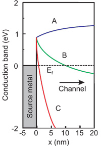 The gate controls the Schottky diode formed at the interface between source metal and the GaN/AlGaN 2DEG channel. At zero bias, the Schottky barrier width (SBW) is about 10nm, according to simulations. The height of the SB is ~0.8eV. As the gate bias is increased, the SBW thins — for example, the SBW is only 1nm with a bias of 3V. This allows a significant increase in tunneling current. The thinning occurs because the gate bias pulls the GaN conduction band down (Figure 2).
Figure 2: One-dimensional plots of simulated conduction-band energy distribution profile of the TJ-FET with source-drain (VDS) voltage of 10V and source-gate (VGS) voltages of –3V (A), 0V (B), and 3V (C).
The researchers also see the reverse current blocking of the Schottky source–channel structure as being beneficial. At large positive drain bias, the Schottky junction is reverse biased. This should suppress leakage through the buffer layer, compared with conventional ohmic source HEMTs.
The devices that were produced had a gate length of 2μm and gate–drain spacing of 2μm. The device demonstrates an on–off current ratio of 1010 — four orders of magnitude better than that (106) for a traditional (normally-on) HEMT (Figure 3). This is achieved through the much lower leakage current in the TJ-FET arrangement. Even at 50V drain bias, the leakage is of the order of 10–8mA/mm.
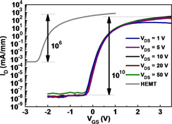 Figure 3: Experimentally measured ID–VGS transfer characteristics of a TJ-FET at VDS = 1 to 50V. Transfer characteristics of conventional (normally-on) HEMT fabricated on same wafer are measured at VDS = 10V and plotted for reference.
The threshold voltage of the TJ-FET is 1.35V. With a source–drain voltage of 10V, the drain current is 326mA/mm at a gate voltage of 3.5V. The transconductance (Gm) is in the range 130–135mS/mm for gate voltages of 2–3.5V. This indicates ‘excellent’ linearity when the device is turned on.
The subthreshold behavior is also sharper. Comparisons between a TJ-FET and a conventional HEMT on the same wafer gave a subthreshold slope (SS) of 89mV/dec for zero drain voltage for the TJ-FET, compared with ~120mV/dec for the HEMT. At 50V drain voltage, the TJ-FET SS was less than 100mV/dec, while the HEMT value was ~125mV/dec.
The researchers comment: “The TJ-FET shows significantly lower SS than the conventional HEMT due to the sensitive tunnel-current-controlling mechanism by the effective barrier thickness of the source Schottky junction.”
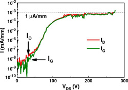 The researchers also determined three-terminal breakdown characteristics at a negative gate voltage of –1V (Figure 4). The researchers compared gate and drain leakage. At less than 70V drain bias, the current leakage was predominantly through the source–buffer reverse-bias Schottky junction. Above this drain bias, the leakage is mainly from the gate through the Al2O3 layer. Hard breakdown was reached at 274V, which compares with 117V for the conventional HEMT.
Figure 4. Measured three-terminal OFF-state breakdown characteristics of a TJ-FET at VGS = –1V.
The specific on-resistance of the TJ-FET was 0.69mΩ-cm2, including the area of the ohmic drain.
Ohio boosts nitride tunneling current to 118A/cm2 at –1V
AlGaN/GaN Tunnel-Junction FETs
The author Mike Cooke is a freelance technology journalist who has worked in the semiconductor and advanced technology sectors since 1997.