- News
21 March 2011
Polarization junctions increase nitride transistor breakdown voltage
Researchers from the UK’s University of Sheffield and Japanese firm POWDEC K.K. have demonstrated super heterojunction field-effect transistors (HFETs) based on polarization junctions “for the first time” [Akira Nakajima et al, IEEE Electron Device Letters, published online 14 February 2011]. One super HFET that was produced had a breakdown voltage in excess of 1.1kV without the use of the field plates that are often used to massage the electric field distribution in such devices.
The researchers are aiming to develop technology for next-generation ultra-low-loss power devices beyond the GaN material limit. They see lateral devices as being “ideally suited for ultra-high-efficiency power ICs with small chip size”.
The new Sheffield/POWDEC device applies a polarization technique to create two-dimensional gases of both electrons (2DEG) and holes (2DHG), reported late last year by the same researchers (Two-dimensional hole gas with increased density and mobility). The concept has also been applied to nitride semiconductor diodes, where operation was maintained up to 9kV.
Often the polarization fields resulting from the ionic nature of III-nitride materials can impede device performance in light-emitting devices. However, in HFETs these polarization electric fields that arise from the different polarization properties of the heterostructure layers also create the 2DEG channels on which conduction between source and drain depends. When the conduction is solely through electrons, these devices can also be referred to as high-electron-mobility transistors (HEMTs).
In the Sheffield/POWDEC device (Figure 1) the polarization fields arise at the interfaces between undoped aluminum gallium nitride (AlGaN) and gallium nitride (GaN) layers. By having two compensating interfaces in the GaN/AlGaN/GaN sequence, the OFF-state can be maintained to higher source–drain bias. “During the OFF state, these positive and negative charge quantities balance each other to result in a flat electric field distribution to maximize the breakdown voltage,” the researchers write.
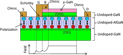
Figure 1: Schematic of Sheffield/POWDEC super HFET and the electric field distribution in OFF-state. There are four electrodes of source (S), gate (G), base (B), and drain (D). The base is electrically connected to the gate. The 2DHG is charged and discharged during the switching cycle through the base electrode.
The ON-state flow occurs through the 2DEG, as in conventional HEMTs. However, in the turn-off stage, the 2DEG is removed through the drain and the 2DHG through the base electrode. The drift region between the base and drain electrodes is thus depleted. On increasing the drain bias a flat field is maintained in the drift region, improving the breakdown capability of the device.
The researchers see their structure as being analogous to the reduced surface field (RESURF) technique used in silicon high-power devices. RESURF uses a ‘drift’ region between the gate and drain to reduce the field in lateral devices, allowing higher voltages to be applied before the critical electric field is reached.
The researchers produced both conventional and the new super HFETs on the same sapphire wafer, using metal-organic chemical vapor deposition (MOCVD). For the conventional HFETs, the p- and undoped-GaN layers were completely removed by using inductive coupled plasma etching. The ohmic source drain contacts consisted of 800°C annealed titanium-aluminum-titanium-gold layers. The Schottky gate and ohmic base contact consisted of 600°C annealed nickel-gold on AlGaN and p-GaN, respectively. A 300nm silicon dioxide layer provided passivation.
The gate–source distances were 3μm for both devices. The gate–drain distance for the conventional device was 10μm; two gate–drain distances of 10μm and 22μm were produced for the super HFET. The base contact measured 4μm. The distance between the GaN layers and the drain of the super HFET was 3μm.
The 10μm gate–drain devices had similar performance in terms of ON-resistance. The longer 22μm gate–drain distance increased the ON-resistance of the super HFET from an RON.A value of 2.2mΩ-cm2 (10μm value) to 6.1mΩ-cm2. There is generally a trade-off between specific ON-resistance and breakdown voltage. The maximum drain current of the 10μm device was 0.29A/mm at a gate voltage of +2V.
The peak transconductance of the super HFET (62mS/mm) was depressed relative to the conventional device (81mS/mm) due to the effective gate length being longer in the super HFET since the base contact was electrically connected to the gate.
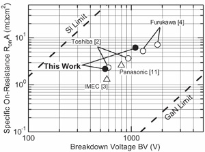 The breakdown performance (Figure 2) was demonstrated at a gate voltage of –15V (OFF-state) with a drain current of 10μA/mm indicating breakdown. The form of the breakdown curves suggested an avalanche mechanism between the gate and drain.
Figure 2: Specific ON-resistance versus breakdown voltage of GaN devices with D-mode (circle) and E-mode operation (triangle). The dashed lines are theoretical material limits of Si and GaN unipolar devices.
The conventional device breakdown voltage (BV) occurred at 100V, lower than the results found with HFETs using field-plates. Without the field-plate, the breakdown tends to occur at the gate edge of the drain side due to electric field crowding. The researchers also suggest that damage from the plasma etch used to remove the p-/u-GaN layers not wanted for the conventional devices may have contributed to increased leakage current effects.
The 10μm super HFET had a breakdown of 560V, and that of the 22μm device exceeded that of the measurement system (1.1kV).
The researchers comment: “The BV of super HFETs is significantly enhanced due to charge compensation effect between the positive and negative polarization charges”. Since the RON.A is almost comparable with previously reported conventional HFETs with field-plates, “further improvement can be expected by optimizing the device structure.”
HFET MOCVD Two-dimensional hole gas AlGaN GaN HEMTs
The author Mike Cooke is a freelance technology journalist who has worked in the semiconductor and advanced technology sectors since 1997.
Join Semiconductor Today's LinkedIn networking and discussion group