- News
13 September 2011
Deep ultraviolet goes deeper on silicon
Japan-based researchers have produced 256–278nm deep ultraviolet (DUV, shorter than 300nm or 350nm, according to taste) light-emitting diodes on silicon substrates [Takuya Mino et al, Appl. Phys. Express, vol4, p092104, 2011]. The organizations involved were Japan’s Institute of Physical and Chemical Research (RIKEN), Panasonic Electric Works Co Ltd, and the University of Tokyo.
Potential applications for DUV devices include sterilization, water purification, medicine, and biochemistry. Advantages of growing devices on silicon substrates include low-cost, large-diameter wafers, electrical conductivity control, and good thermal conductivity. The Japan-based researchers also see possibilities for low-cost AlGaN-based DUV LEDs on Si substrates to be integrated with Si-based electrical circuits on the same chip.
To maximize the amount of light produced by LEDs, one has to increase the internal quantum efficiency (IQE) of electricity in producing photons, along with optimizing the light extraction efficiency (LEE) to give high external quantum efficiency (EQE), the desired final product.
The Japanese research focused on improving IQE through improved crystal quality, in particular, of the initial aluminum nitride (AlN) template layer, since IQE is adversely affected by the presence of threading dislocations. For DUV devices using nitride semiconductor layers, one of the key factors is the large lattice mismatch of about 19% between (0001) AlN and Si oriented with a (111) surface. The mismatch is even worse — about 43% — between AlN and the (100) Si used in most CMOS production.
Lattice mismatch increases the number of threading dislocations (TDs). Another problematic factor is the difference in thermal expansion between AlN and Si that leads to cracking of the crystal material when layers are cooled from growth (1300°C) to room temperature (~20°C).
The Japanese DUV LEDs were grown on (111) silicon wafers using metal-organic chemical vapor deposition (MOCVD) with trimethyl-metal and ammonia sources for the gallium/aluminum and nitrogen, respectively.
AlN template layers were grown at 1300°C in two steps: first, using a pulsed ammonia flow, and then a continuous flow. The second step relaxes the tensile stress in the AlN. When the second step is not used, one finds cracked surfaces.
The first step produced 300nm AlN layers that were then patterned for epitaxial lateral overgrowth (ELO) by etching with inductively coupled plasma down to the silicon with 2μm wide linear grooves separated by 8μm wide terraces. ELO reduces the area from which subsequent nitride crystal material is seeded for further growth, hence reducing stress and the number of TDs. Different directions for the grooves were tried along the <11-20> and <10-10> directions.
The ELO layer consisted of continuous-flow AlN growth performed at 1300°C to give a total thickness of 4μm with the 300nm seed layer.
A series of optical and electron microscopic examinations were performed, along with x-ray diffraction. It was found that the <11-20> material from adjacent strips did not coalesce well, so further work focused on the <10-10> material that did coalesce successfully. Although some cracking was observed on the surface of the <10-10> material, the researchers comment that “ELO-AlN is effective for relaxing the tensile stress generated by the mismatch in the lattice and thermal expansion coefficients between AlN and Si, because a 4μm-thick AlN layer on Si would crack heavily without the ELO-AlN layer.”
Transmission electron micrography (TEM) was used to estimate the threading dislocation densities as 2x10⁸/cm2 for screw-type and 9.5x10⁸/cm2 for edge-type. X-ray diffraction rocking curves confirmed improved crystal quality with full-width at half maximum (FWHM) values of 780arcsec and 980arcsec for the (0002) and (10-12) peaks, respectively. These compare, respectively, with the values for the initial 300nm AlN layer of 3500arcsec and 3750arcsec. The researchers comment that the (10-12) FWHM value of 980arcsec “is lower than that of AlN templates on Si reported so far”.
One of the researchers, Hideki Hirayama, had previously worked on the pulsed-flow technique for producing AlN on Si at RIKEN with Sachie Fujikawa, producing 280–300nm devices on silicon using InAlGaN active light-emitting layers. The produced AlN was 200nm after pulsing and 2μm in total after the second step. In this previous work, no ELO patterning was used and the (10-12) rocking curve FWHM was 2000arcsec.
The DUV LEDs (Figure 1) were produced using LP-MOCVD on AlN templates on Si with <10-10> trenches. The three-layer multi-quantum well (MQW) active region consisted of undoped AlGaN 1.5nm wells and 6nm barriers. The aluminum content of the wells varied between 40% and 55%, while the barriers had 70%, like the n-AlGaN region. An electron-blocking layer (EBL) was used to avoid IQE losses from overshoot of electrons into the p-type contact region.
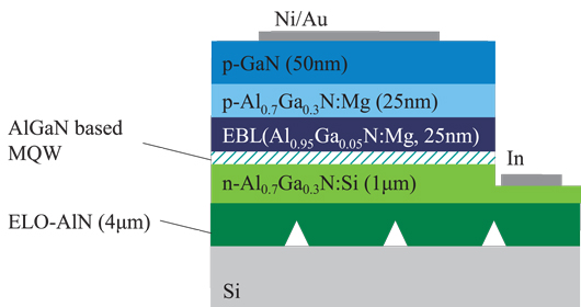
Figure 1: Schematic of AlGaN-based DUV LED fabricated on <10-10>-trench-patterned ELO-AlN/Si template on a Si substrate.
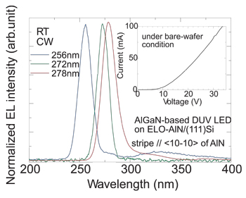 Continuous-wave emission was measured using bare wafers at room temperature in an integrating sphere (Figure 2). The forward voltages at 1mA and 20mA were 7V and 16V, respectively. The relatively high voltages are attributed to series resistance from lateral injection in the n-type layer. The researchers comment: “The forward voltage will be significantly reduced by using a flip-chip packaged device or by using a vertical LED structure by removing the Si substrate and AlN buffer”.
Figure 2: Electroluminescence spectra and typical current–voltage (I–V) curve of AlGaN-based DUV LEDs on ELO-AlN templates on Si at room temperature.
The output powers are three orders of magnitude lower (i.e. a factor of a thousand) than those found for DUV devices grown on sapphire. At 500mA, a typical device produced 10μW, compared with more than 10mW found for some sapphire-based devices.
One problem with using silicon substrates is that silicon absorbs the DUV emission, so the emitted light can only be extracted from the top. Sapphire is transparent to DUV and most DUV LEDs use a flip-chip arrangement, extracting the light through the bottom of the device. A further loss occurs through absorption in the p-GaN contact layer. The researchers estimate that 85% of the light travelling in the upward direction is lost in this way.
Unfortunately, a p-GaN contact is needed at present in DUV devices because the magnesium doping used to create p-type conduction in nitride semiconductors has a high activation energy that increases with high Al-content. High activation energies lead to low hole concentrations. For example, the researchers estimate that the hole concentration in the p-GaN layers of their devices is about 1017/cm3, compared with 1014/cm3 in the p-AlGaN EBL. By contrast, the silicon doping used to create n-type conduction has a low activation, resulting in an electron concentration in the n-AlGaN layer of 1018/cm3.
In addition to all these problems, more light is blocked by the nickel-gold p-electrode.
The researchers estimate that their present structure has a light extraction efficiency (LEE) of 0.01%. An improved LEE of 10% could result from removal of the Si substrate and the use of a vertical current-flow flip-chip structure.
Simulating way to improved DUV LEDs
Liquid phase pushes deep ultraviolet to higher efficiency
Lateral conduction, substrate-free deep UV nitride semiconductor LEDs
http://apex.jsap.jp/link?APEX/4/092104