

- News
11 December 2012
Polystyrene nanospheres focus effort on photonic crystal for nitride LED
Researchers in China have developed a low-cost, high-throughput photonic crystal (PhC) process for nitride semiconductor light-emitting diodes (LEDs) [Tongbo Wei et al, Appl. Phys. Lett., vol101, p211111, 2012]. The process used nanospherical-lens photolithography (NLP) and re-growth of gallium nitride to improve light extraction from and generation in the LEDs.
The nanospheres consisted of polystyrene. Some of the same researchers have previously used polystyrene nanospheres to create surface texturing of nitride LEDs for improved light extraction [e.g. Vertical-stand surface-roughened nitride LEDs with 118.5% increased output. The researchers of the latest work were based at Chinese Academy of Sciences’ institutes of Semiconductors and of Mechanics, and Tsinghua University.
‘Photonic crystals’ are periodic structural arrays that can alter optical properties of materials such as light extraction through interfaces. The interface between flat gallium nitride (GaN) and the air suffers from a particularly small escape cone of ~24° due to a large ratio of refractive indices (~2.5:1).
Proposed processes for creating PhCs tend to be time consuming/low throughput. The new process uses self-assembled arrays of nanospheres to focus light rather than a lithographic technique using masks (Figure 1).
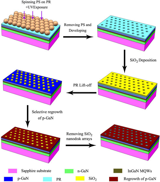
Figure 1: Process schematic for fabricating SiO2 PhC LEDs and air-hole PhC LEDs by NLP method.
Blue indium gallium nitride (InGaN) LED structures were grown on c-plane sapphire using metal-organic chemical vapor deposition (MOCVD). The active region consisted of 8-period multi-quantum wells (MQWs) with In0.2Ga0.8 wells and GaN barriers. The PhC was formed on the 100nm p-GaN top layer (Figure 1) using NLP.
The NLP process consists of using the hexagonally close-packed array of polystyrene nanospheres as lenses to selectively expose underlying AR-P 3120 photoresist (PR) to UV radiation. The nanosphere layer was then removed through ultrasound exposure in deionized water.
The PR pattern was developed and used as a mask for ion-beam sputtering deposition of 150nm silicon dioxide (SiO2). The size of the holes in the PR pattern could be controlled by varying the development time. The 900nm or 700nm periodicity of the holes was determined by the nanosphere size.
| PhC | Periodicity | Forward voltage | Light output power enhancement | Wall-plug efficiency enhancement | Peak wavelength | Angular divergence (full-width at half-maximum) |
| None | 0 | 3.15V | 0% (reference) | 0% (reference) | 447.6nm | 151.3° |
| SiO2 | 900nm | 3.23V | 71.3% | 67.1% | 442.4nm | 137.8° |
| SiO2 | 700nm | 4.37V | 83.8% | 32.2% | 445.9nm | 132.5° |
| Air | 900nm | 3.21V | 49.3% | 46.4% | 441.3nm | 143.2° |
| Air | 700nm | 3.51V | 67.7% | 50.5% | 444.1nm | 138.6° |
Table 1: LED performance characteristics at 350mA injection current, except for angular divergence measured at 200mA.
The lift-off process consisted of dissolving the PR in acetone, leaving an array of ~450nm-diameter SiO2 nanodisks. The gaps between the nanodisks were filled by further growth (‘re-growth’) of 150nm p-GaN.
An air-hole PhC LED was also produced by wet etch of the SiO2, using hydrofluoric acid. The epitaxial material was formed into conventional 1mm x 1mm mesa nitride semiconductor LEDs with a 200nm indium tin oxide (ITO) current-spreading layer, and chromium/platinum/gold n- and p-electrodes.
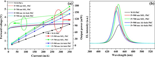
Figure 2: (a) Forward voltages and light output powers of LEDs with and without PhC structures as functions of injection current. (b) Peak wavelengths of electroluminescence spectra of LEDs at driving current of 350mA.
The flatness of the p-GaN was affected by the periodicity of the nanodiscs. The larger periodicity resulted in a flat surface, while the 700nm periodicity resulted in bowl-shaped p-GaN around the disks due to the smaller space between nanodisks leading to faster growth. This is reflected in the height of re-grown p-GaN being higher (220nm) with 700nm periodicity, compared with 150nm for the 900nm sample.
The forward voltage at 350mA was higher for 700nm periodicity due to non-ohmic contact between the bowl-shaped p-GaN and ITO layers. By contrast, the 900nm periodicity resulted in negligible degradation in electrical performance, showing the high quality of the flat re-grown p-GaN.
The higher light output enhancement of SiO2 PhC compared with air-hole PhC LEDs was attributed to the bigger incident angle of the PhC Bragg diffraction, introducing SiO2’s refractive index between the p-GaN and air ambient. The additional enhancement of the 700nm periodicity was related to diffused light scattering from the bowl-shaped GaN with inclined facets.
The emission peaks were blue-shifted compared with conventional LEDs (i.e. without PhC), due to partial compression strain release in the InGaN active region as a result of the selective area epitaxial (SAE) re-growth of p-GaN. The compression strain is somewhat higher with 700nm periodicity due to the high growth rate within the constricted space between nanodisks. Removing the nanodisks to give air-holes releases some further strain within the structure.
The angular divergence of the light was also measured on devices on aluminium-leaded chip carrier with gold-wire bonding but without epoxy encapsulation. The larger divergent angle seen for conventional devices was attributed to multiple scattering events. The longer that light is trapped in the device, the more likely it is to be reabsorbed. The presence of the PhC is thought to effectively re-direct light into the top escape cone of the LED through the nanodisks.
The 700nm SiO2 PhC has the best performance in terms of concentrating the light into a smaller angle. The researchers attribute this to the combination of the PhC and the bowl-shaped GaN top surface.
“Unlike the random scattering of surface roughness, the bowl-shaped p-GaN helps to confine the light to radiate in the vertical direction, effectively reducing the energy confined in the LED slab,” the researchers comment.
http://link.aip.org/link/doi/10.1063/1.4767334
The author Mike Cooke is a freelance technology journalist who has worked in the semiconductor and advanced technology sectors since 1997.