- News
13 January 2012
Osram’s GaN LED chips on 150mm silicon enter pilot stage
Researchers at Osram Opto Semiconductors GmbH of Regensburg, Germany have fabricated high-performance blue and white LED prototypes in which the light-emitting gallium nitride (GaN) layers are grown on 150mm-diameter silicon wafers. The silicon wafers replace the sapphire substrates commonly used in the industry, with no loss of quality, it is reckoned. Already in the pilot stage, the new LED chips are being tested under practical conditions, so Osram Opto’s first LEDs on silicon could enter the market in as little as two years.
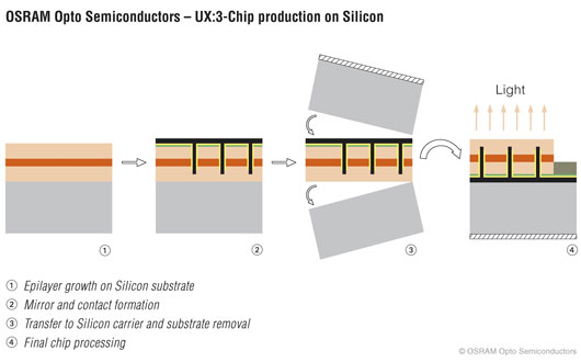
Graphic: Process diagram showing production of a UX:3 chip on a silicon wafer.
Due to its already widespread use in the semiconductor industry, the availability of large wafer diameters and its very good thermal properties, silicon is an attractive and low-cost option for large-volume fabrication, particularly for future lighting markets, says Osram. Quality and performance data on the fabricated GaN-on-silicon LED chips match those of sapphire-based chips: the blue UX:3 chips (measuring 1mm²) in Osram’s standard Golden Dragon Plus package achieve what is claimed to be a record brightness of 634mW at 3.15V when driven at a current of 350mA, equivalent to 58% efficiency. In combination with a conventional phosphor converter in a standard housing (i.e. as a white LEDs) these prototypes correspond to 140lm at 350mA with an efficiency of 127lm/W at 4500K.
“For these LEDs to become widely established in lighting, the component cost must come down significantly while maintaining the same level of quality and performance,” says project manager Dr Peter Stauss. “We are developing new methods along the entire technology chain for this purpose, from chip technology to production processes and housing technology,” he adds. “Mathematically speaking, it is already possible today to fabricate over 17,000 LED chips of 1mm² in size on a 150mm wafer. Larger silicon wafers could increase productivity even more; researchers have already demonstrated the first structures on 200mm substrates.
Osram Opto says that it has acquired comprehensive expertise in the fundamental epitaxial growth technology over the last 30 years. The German Federal Ministry of Education and Research funds these activities as part of its ‘GaNonSi’ project network. “Our investments in years of research are paying off, because we have succeeded in optimizing the quality of the GaN layers on the silicon substrates to the point where efficiency and brightness have reached competitive market levels,” notes Stauss. “Stress tests we've already conducted demonstrate the high quality and durability of the LEDs,” he adds.
Bridgelux raises GaN-on-Si LED efficiency record
High-brightness nitride LEDs on silicon through wafer bonding
Bridgelux claims first commercial-grade performance for Si-based LED