- News
19 March 2012
MOCVD produces high-performance mHEMTs on Si substrates
Hong Kong University of Science and Technology (HKUST) has produced high-performance gallium indium arsenide (GaInAs) metamorphic high-electron-mobility transistors (mHEMTs) on silicon substrates using metal-organic chemical vapor deposition (MOCVD) [Ming Li et al, IEEE Electron Device Letters, published online 7 March 2012].
The researchers sees the devices as “one of the most promising device candidates for future high-speed and low-power digital logic applications”. Further, “Seamless robust heterogeneous integration of high-performance GaInAs transistors on Si will help realize the ultimate vision of low-voltage high-speed III–V-based logic circuit blocks coupled with the functional density advantages provided by the Si CMOS”.
Previous high-performance mHEMTs on Si have been produced using molecular beam epitaxy (MBE), which is less attractive as a mass manufacturing technique. Such devices offer an order of magnitude improvement in energy–delay product, with performance parameters comparable with mHEMTs produced on gallium arsenide (GaAs) or indium phosphide (InP) substrates.
The new devices show similar performance over a range of parameters (Table 1). The researchers comment: “To our best knowledge, these results are the best reported for MOCVD-grown mHEMTs on Si.”
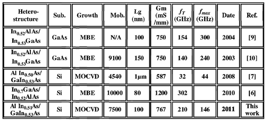
Table 1: Comparison of AlInAs/GaInAs HEMT performance with various production techniques.
The HKUST epitaxial structures were grown on exact (001)-oriented silicon substrates using Aixtron’s AIX-200/4 system (Figure 1). The GaInAs channel and aluminum indium arsenide (AlInAs) barrier layers were lattice matched to InP. The metamorphic buffer was grown using alternating low- temperature (LT) and high-temperature (HT) steps.
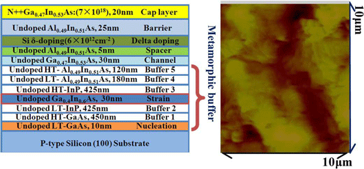
Figure 1: Nominal structure of mHEMT device on Si substrate and atomic force microscope (AFM) image of 10μm x 10μm scan area of buffer structure on Si substrate.
The mHEMT devices were mesa-isolated with ohmic source/drain contacts consisting of nickel/germanium/gold/germanium/nickel/gold. The source–drain spacing was 3μm.
Silicon nitride was deposited using plasma-enhanced CVD and a gate length of 100nm was defined. Various wet etching steps were performed to create a T-gate structure with its foot on the AlInAs barrier layer. The Schottky gate contact consisted of titanium/platinum/gold. The gate width was 400nm.
The maximum extrinsic transconductance of the resulting device was 767mS/mm. The threshold voltage was negative, -0.45V, giving depletion/normally-on behavior. Below threshold, at -1.2V gate potential, the current was less than 0.32mA/mm at 1V drain bias. The gate leakage current of 0.12mA/mm at a gate potential of -3V and a drain bias of 1V was lower than previous work, due to the high resistivity of the multi-stage metamorphic buffer scheme.
The frequency performance of the device was tested in the range 0.1-39.1GHz, giving extrapolations for the cut-off frequency (fT) of 210GHz and for the maximum oscillation frequency
(fmax) of 146GHz.
The researchers comment that they expect enhanced RF performance with improved fabrication techniques. “These results are very encouraging toward the manufacturing of high-performance metamorphic devices on Si substrates by MOCVD,” they say.
High-performance 150nm mHEMT on GaAs grown using MOCVD
GaInAs mHEMTs MOCVD Si substrates
The author Mike Cooke is a freelance technology journalist who has worked in the semiconductor and advanced technology sectors since 1997.