- News
9 May 2012
Plasma oxidation of aluminium for insulated nitride transistor gates
RWTH Aachen University and Aixtron SE in Germany have developed a new technique to create aluminium oxide insulated gates for nitride semiconductor transistors [Herwig Hahn et al, Semicond. Sci. Technol., vol27, p062001, 2012]. The method consists of depositing a thin layer of aluminium that is then oxidized in oxygen plasma, creating an insulating layer of aluminium oxide (AlOx).
Nitride transistors have excellent potential as the basis of RF power amplifiers and are also promising for use in high-power switches. However, at present, gate leakage currents limit the lifetime and performance of such devices. These currents are relatively high because up to now the best performing devices have used a gate with metal deposited directly on the nitride semiconductor material, using the rectifying Schottky barrier as insulation. This only works in the range of the Schottky barrier height.
 For power devices, one tends to want enhancement-mode (e-mode) devices that are normally off when there is no gate potential, reducing power consumption and allowing fail-safe operation. Such e-mode devices should need high positive gate voltages for significant drain current to flow. However, such potentials would then be near or fall outside the Schottky barrier height.
Recently, researchers around the world have been searching for a way to incorporate an insulation layer between the gate and channel, in the same way as in metal-oxide-semiconductor field effect transistors (MOSFETs).
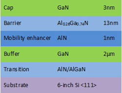
Figure 1: Layer sequence of aluminium gallium nitride (AlGaN) epitaxial materials with 420Ω/square sheet resistance and sheet charge density 6.5x10¹²/cm2.
The epitaxial material (Figure 1) used by RWTH/Aixtron was grown using metal-organic chemical vapor deposition (MOCVD) on 6-inch silicon (Si) <111> substrates. The material was diced into 15mm x 15mm pieces. Circular large-area diodes and transistors were used to test the gate formation process (Table 1).
Sample |
Preparation |
Ref. |
Ni/Au gate stack |
A |
Al/Ni/Au evaporated at once |
B |
Al exposed to clean room air for 1 h |
C |
Al plasma-oxidized for 2 min, −20 V RF bias |
D |
Al plasma-oxidized for 10 min, −50 V RF bias |
Table 1: Set of Schottky reference and four samples with variation in processing of Al layer.
The 50nm/200nm nickel/gold (Ni/Au) reference represents a standard Schottky gate structure. Sample A consisted of 3.5nm aluminium applied before further evaporation of Ni/Au gate metals of the same thickness as for the reference. Samples B, C and D were subjected to oxygen in various forms.
The plasma oxidations were carried out in the chambers of equipment designed for inductively coupled plasma reactive ion etching (ICP-RIE). After oxidation, the samples were returned to the evaporation equipment for further metal deposition of 50nm/200nm Ni/Au.
The gates were deposited on photoresist masks that were later removed in a standard lift-off process. The 2μm gate-length transistors also had standard ohmic contacts for the source/drain access applied before gate deposition. Various 10-minute rapid thermal anneal treatments in nitrogen were explored.
The diode measurements suggested that an aluminium oxide (AlOx) dielectric layer had formed in sample D with a capacitance of 1130nF/cm2. Assuming a typical dielectric constant of 9 would give a layer thickness of 7nm. The reverse gate leakage was 10–4A/cm2, at least one order of magnitude smaller than that of the standard Ni/Au Schottky gate of the reference sample. Sample C also showed the presence of a dielectric, but had a higher reverse gate leakage of 0.01A/cm2.
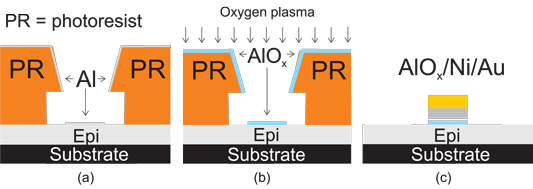
Figure 2: Process scheme for samples C and D. First, Al was evaporated (a). Second, the samples were exposed to oxygen plasma in an ICP tool (b). Third, Ni and Au were evaporated with subsequent lift-off (c).
Since the other samples showed significant degradation due to the presence of interface trap states, the researchers concentrated on sample D in further anneal processing and measurements. Annealing at 600°C reduced gate leakage by an order of magnitude. In transistor structures, the same anneal process resulted in gate leakage less than 1nA/mm, raising the prospect of on/off ratios of the order of 109.
Capacitance–voltage measurements at 1MHz show a fall in capacitance with increasing anneal temperature. The researchers comment: “With the decreasing capacitance, the formation of oxides with lower dielectric constant has to be assumed. Also, a reaction with the GaN cap layer cannot be excluded. At the moment, no reasonable explanation for this effect can be presented and, due to this, a meaningful estimation of the oxide thickness cannot be performed.”
Also, shifts in the threshold voltage were found with different anneal temperatures. Unusually the shift was in the positive direction, despite reduced capacitance that would normally be expected to give a negative trend.
For transistors (Figure 3a), another effect of increased anneal temperature is reduced subthreshold swing (steeper slope). For 600°C annealing, the swing is reduced to 80meV/dec, close to the room-temperature limit of 60meV/dec. Again, the threshold increases by +0.7V. The transconductance is increased from 80mS/mm for the as-deposited sample to almost double at 140mS/mm for 600°C annealing. The researchers see the transconductance as “quite good” for unpassivated devices with a thick AlGaN barrier and 2μm gate length.
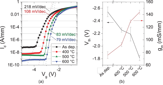
Figure 3: Semi-logarithmic transfer characteristics for 10V drain bias (a) and dependence of threshold voltage (left) and peak transconductance (right) vs annealing temperature (b).
The researchers find that the transconductance improvement is associated with the subthreshold performance, “indicating a better controllability of the channel due to a decreased amount of trap states at the insulator–semiconductor interface”, and not to reduced source resistance.
The researchers conclude: “As this process is applicable with surface passivation prior to gate deposition, it might be an elegant way to form high-performance enhancement-mode MISHFETs.”
More polarization engineering enhancement in nitride semi HFETs
Polarization matching as a route to nitride semiconductor transistor enhancement
RWTH Aachen Aixtron GaN AlN AlGaN MOCVD MISHFETs
The author Mike Cooke is a freelance technology journalist who has worked in the semiconductor and advanced technology sectors since 1997.