- News
21 May 2012
Selective area growth recessing for improved normally-off nitride HFETs
Researchers in China based at State Key Laboratory of Optoelectronic Materials and Technologies, Sun Yat-Sen University, have demonstrated a selective area growth (SAG) method for recessing gates in aluminium gallium nitride (AlGaN) semiconductor heterostructure field-effect transistors (HFETs) [Zhiyuan He et al, Jpn. J. Appl. Phys., vol51, p054103, 2012]. The resulting device had higher performance than one produced using conventional recessing techniques by avoiding the damage associated with plasma etch.
Recessing refers to the creation of a trench in the barrier layer of the HFET, reducing the distance between the gate electrode and channel. This can shift the threshold voltage of the transistor in a positive direction, even enabling normally-off behavior (off at zero gate potential) as opposed to the usual normally-on operation of simple nitride HFETs. Normally-off operation is desirable for reducing power consumption and for fail-safe operation in power devices.
The HFET structures (Figure 1) were grown on silicon (111) substrates using metal-organic chemical vapor deposition (MOCVD). The buffer consisted of 1.4μm of high-resistance intrinsic GaN. The barrier layer was Al0.25Ga0.75N. The SAG process for recessing consisted of patterning a silicon dioxide mask layer on top of a 10nm AlGaN barrier. A further 15nm growth was then carried out to leave a recessed stripe for the gate electode.
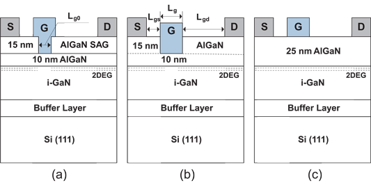
Figure 1: Schematics of SAG-HFET (a), ICP-HFET (b) and C-HFET (c).
Comparison devices with (ICP-HFET) and without (C-HFET) recessing from inductively coupled plasma (ICP) etch into the 25nm AlGaN barrier layer were also produced.
The devices were isolated with mesa etching. The ohmic source-drain contacts consisted of 830°C-annealed titanium/aluminum/nickel/gold. The gates consisted of nickel/gold Schottky contacts. The gate length was 3μm. The gate-source and gate-drain distances were 1.5μm and 4μm, respectively. The gate width was 15μm.
The ICP- and SAG-HFETs demonstrated positive thresholds of 0.6V and 0.4V with maximum drain currents at 6V bias of 64mA/mm and 300mA/mm, respectively. The C-HFET had larger maximum drain current of 750mA/mm due to the higher density of carriers under the gate.
The researchers estimated the gate injection current into the channel at +1.6x10⁻⁴mA/mm,
+1.3x10⁻⁴mA/mm and +48.4mA/mm for the C-, SAG, and ICP-HFETs, respectively. The high injection for the ICP-HFET indicates that the Schottky diode gate has turned on, losing its ability to control current flow in the channel. Under positive gate voltage, the electrons from the source end up in the gate and not the drain of the ICP-HFET, resulting in the poor maximum drain current.
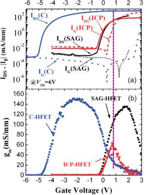 The extrinsic (i.e. uncorrected for source resistance effects) transconductance performance gave peak values of 150mS/mm, 135mS/mm and 64mS/mm, respectively, for the C-HFET, SAG-HFET and ICP-HFET devices. The corresponding intrinsic (corrected) transconductances were 234mS/mm, 356mS/mm and 90mS/mm.
Figure 2: (a) Gate and drain currents under drain voltage of 6V, and (b) transconductance characteristics, for the three HFETs; the value for ICP-HFET showed a sudden drop when the gate voltage increased beyond 1V, corresponding to a sharp increase in gate forward current (marked with dotted line).
The high intrinsic transconductance of the SAG-HFET is probably due to the recessed gate being closer to the channel, giving greater control compared with the C-HFET. The ICP-HFET suffers from the gate leakage current that kicks in before the peak is reached with the SAG-HFET (Figure 2).
Pinch-off current leakage at a negative gate potential of -5.5V and drain bias 20V was
-1.6x10⁻³mA/mm, -2.0x10⁻²mA/mm and -2.2x10⁻³mA/mm, for C-, ICP- and SAG-HFETs, respectively. Again, the ICP-HFET showed (an order of magnitude) worse behavior.
The researchers believe that the ICP-HFET Schottky contact is degraded by the plasma etch process, where crystal damage could create defects that allow barrier tunneling effects.
More polarization engineering enhancement in nitride semi HFETs
The author Mike Cooke is a freelance technology journalist who has worked in the semiconductor and advanced technology sectors since 1997.