- News
11 May 2012
Record transconductance of 1105mS/mm for GaN/InAlN MIS-HFET
University of California Santa Barbara (UCSB) has produced gate-first self-aligned metal-insulator-semiconductor heterostructure field-effect transistors (MIS-HFETs) based on nitride semiconductors that demonstrated record extrinsic transconductance of 1105mS/mm [Nidhi et al, IEEE Electron Device Letters, published online 26 April 2012].
The devices used N-polar nitride semiconductor material rather than the more usual Ga-polar gallium nitride (GaN) buffer devices. Also, instead of a strained aluminium gallium nitride (AlGaN) top barrier, the UCSB devices use an unstrained indium aluminium nitride (InAlN) bottom/back barrier to generate a two-dimensional electron gas (2DEG) in the GaN channel layer.
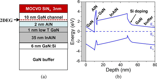
Figure 1: (a) Device epitaxial-layer structure for scaled GaN channel with InAlN back barrier. (b) Band diagram of the device under the gate.
The epitaxial material (Figure 1) for the devices was grown using plasma-assisted molecular beam epitaxy (PA-MBE) on C-face 6H silicon carbide (SiC) substrates. The In0.17Al0.83N back-barrier was lattice matched to the GaN layers. The 1nm of low-temperature GaN was designed to inhibit indium desorption in subsequent high-temperature process steps. The 2nm AlN interlayer was aimed at reducing alloy scattering. The structure was found to give a low sheet resistance of 330Ω/square.
A silicon nitride layer was applied as gate dielectric using metal-organic chemical vapor deposition (MOCVD). The gate metal stack consisted of tungsten/chromium/silicon dioxide/chromium. These steps constitute the ‘gate-first’ part of the self-aligned process.
After gate definition, a 40nm layer of silicon nitride layer from plasma-enhanced chemical vapor deposition (PECVD) was used as spacer material around the gates to allow MBE re-growth of highly doped InGaN/InN for source/drain contact access, giving an ‘ultra-low’ contact resistance of 25Ω-μm. The polycrystalline growth on the gate finger was etched away, followed by mesa isolation of the individual transistor. Titanium/gold non-alloyed metal layers were used as source/drain ohmic and probe contacts.
A 60nm-gate device showed a maximum drain current density of 2.77A/mm and an on-resistance of 0.29Ω-mm. The current is described as ‘state-of-the-art’ for both Ga-polar and N-polar devices. The on-resistance is “the lowest value ever reported for a GaN device.”
At 0V gate potential, the saturated drain current was 2.13A/mm at drain bias of 2V. For a 30nm-gate device, the saturated drain current density was 2.25A/mm. The peak extrinsic transconductances (gm) were 1105mS/mm and 1000mS/mm for 60nm and 30nm gates, respectively. The researchers comment: “This is the highest value for extrinsic gm reported for III-nitride HEMTs on any crystal orientation.”
The off-state leakage was around 20mA/mm for 2V drain bias. Hard breakdown occurred at 24V drain bias.
The researchers attributed the improved device performance to “significant reduction in the device to low on-resistance and high extrinsic transconductance.”
The performance was also measured up to frequencies of 67GHz. The 30nm device had a cut-off frequency (fT) of 155GHz, but a maximum oscillation of only 20GHz (drain 3V, gate -2.5V). The poor fmax figure was blamed on the high resistance of the tungsten-gate.
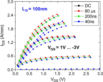 Although the fT is ‘excellent’, it does not reflect what should be expected from the transconductance value, along with the relatively low values for the parasitic components. Pulsed measurements (40nsec), however, showed significant current collapse and ‘knee walkout’ (Figure 2).
Figure 2: Pulsed current–voltage (I–V) characteristics for 100nm gate, showing significant current collapse and knee walkout for 40ns gate pulses.
The researchers tentatively attribute these effects to “shallow traps in the plasma MBE-grown InAlN or the low-temperature GaN layer below the AlN interlayer.”
The UCSB work was supported in part by US Navy and Defense Advanced Research Projects Agency (DARPA) funding.
Plasma oxidation of aluminium for insulated nitride transistor gates
MIS-HFET GaN/InAlN SiC substrates PA-MBE MBE PECVD MOCVD
The author Mike Cooke is a freelance technology journalist who has worked in the semiconductor and advanced technology sectors since 1997.