- News
10 September 2012
First ammonia MBE nitride semi HEMTs on silicon
Singapore’s Nanyang Technological University has made a first demonstration of nitride semiconductor high electron mobility transistors (HEMT) grown on silicon substrates using ammonia molecular beam epitaxy (MBE) rather than the usual metal-organic chemical vapor deposition (MOCVD) or plasma-assisted MBE [Nethaji Dharmarasu et al, Appl. Phys. Express, vol5, p091003, 2012].
While MOCVD has the attraction of high growth rates, MBE methods offers more control of growth parameters and sharper interfaces between layers. Also in situ monitoring of MBE gives growth process control at the monolayer level.
With the rise of commercial interest in growing nitride semiconductors on silicon as opposed expensive silicon carbide or thermally insulating sapphire, further advantages of MBE include lower growth temperature allowing better management of differences in thermal coefficients of expansion. Also, the ultra-high vacuum used for MBE minimizes hydrogen incorporation that impacts the effectiveness of magnesium doping for p-type nitride layers.
The use of ammonia rather than plasma-assisted MBE increases growth rate and the process parameter window for high quality, more uniform material growth. In HEMT applications, the resulting material has lower buffer leakage due to growth in nitrogen-rich rather than metal-rich conditions, giving a high resistance buffer layers. Thus current flow is restricted to the two-dimensional electron gas that forms near barrier/channel interfaces.
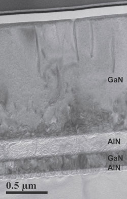 The epitaxial structures were grown on 100mm diameter high-resistivity (more than 10,000Ω-cm) silicon oriented in the (111) direction preferred for nitride semiconductor growth. The layers consisted of 50nm aluminium nitride (AlN) nucleation, 200nm gallium nitride (GaN) and 200nm AlN stress mitigation, variable thickness GaN buffer/channel, 28nm AlGaN (25% Al) barrier, and 2nm GaN cap (Figure 1).
Figure 1: High resolution transmission electron micrograph (HR-TEM) cross-section of GaN/AlN/GaN/AlN/Si(111) structure.
The ammonia molecular beam epitaxy process was optimized with the help of reflection high-energy electron diffraction (RHEED) patterns. The temperature was varied with 750°C used for pre-deposition clean, 800°C for AlN growth and 920°C for GaN growth. Also the growth rate for the stress mitigation layers was tuned to speed the transition from 3D to 2D lateral growth that suppresses defect propagation. An additional improvement from higher growth rates was compressive stress in the GaN layer that balanced thermal-expansion-mismatch-induced tensile stress during cooling. The result was a crack-free buffer layer.
The material was subjected to Hall Effect measurements giving a room temperature (300K) mobility for the two-dimensional electron gas at the AlGaN/GaN interface of 1350cm2/V-s and carrier density of 1.2x10¹³/cm2. The average sheet resistance was 368Ω/square. At 90K, the mobility reached 4290cm2/V-s. By contrast, the carrier density was relatively insensitive to temperature variation over the range 90-400K.
The researchers also assessed buffer leakage. A 1.7μm buffer showed the lowest current of 2.6x10⁻⁴mA/mm at 20V bias, giving an on/off current ratio of 7.3x10⁶. Similar HEMT structures grown using plasma-assisted MBE had buffer leakage values of 1mA/mm and on/off current ratios of 400.
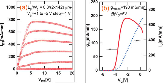
Figure 2: (a) Drain current-voltage characteristics and (b) extrinsic transconductance vs. gate potential transfer characteristics of 0.3μm-gate-length AlGaN/GaN HEMTs.
The researchers characterized a nickel-gold T-gate device with gate length and width of 0.3μm and 2x142μm respectively (Figure 2). The maximum drain current was 768mA/mm at 1V gate potential and the peak extrinsic transconductance 190mS/mm at 6V drain bias. The threshold voltage was -4.53V.
GaN-on-Si large-signal performance beyond 40GHz
Nitride HEMTs grown on CMOS-compatible silicon
Nitride HEMTs Silicon substrates MBE GaN
The author Mike Cooke is a freelance technology journalist who has worked in the semiconductor and advanced technology sectors since 1997.