


- News
15 January 2014
Embedded Schottky diode for unidirection GaN HFET
Korea’s Hongik University has demonstrated a unidirectional nitride semiconductor heterostructure field-effect transistor (HFET) that embeds a reverse current block Schottky diode into the drain contact [Jae-Gil Lee et al, Appl. Phys. Express, vol7, p014101, 2014]. Hongik has previously worked with Cornell University on embedding Schottky diodes to block reverse currents in AlGaN/GaN metal-oxide-semiconductor HFETs - see Embedding diodes in normally-off GaN transistors.
Hongik is seeking to develop devices that could compete with silicon-based power devices such as insulated-gate bipolar transistors (IGBTs) and power metal-oxide-semiconductor field-effect transistors (MOSFETs). Aluminium gallium nitride (AlGaN) compound alloys have higher critical fields, high carrier concentration and high mobility, making these materials attractive for power applications.
Such devices are designed to have high breakdown in the forward direction. Typically, the gate-drain distance is much longer than the source-gate distance. Long gate-drain distances are used to reduce peak electric fields and hence delay breakdown. A negative drain bias would reverse the roles of source and drain, leading to premature breakdown and potential damage of the device, hence the need for a diode to block reverse currents through the device.
Table 1: Epitaxial structure used in unidirectional HFET.
| Cap | GaN | 4nm |
| Barrier | Al0.23Ga0.77N | 20nm |
| Spacer | AlN | 1nm |
| Buffer | GaN | 1.7μm |
| Multilayer | GaN/AlN | 3.7μm |
| Transition | AlN-rich | 0.4μm |
| Substrate | (111) n-Si |
The new Hongik device used an epitaxial structure on n-type silicon (n-Si) with AlGaN alloy barrier layer (Table 1).
The fabrication of HFETs with a Schottky contact (Figure 1) included mesa etch for isolation, silicon/titanium/aluminium/molybdenum/gold ohmic metal deposition and annealing for the source/drain contacts, silicon dioxide surface passivation, and gate formation by buffered oxide etch and nickel/gold deposition.
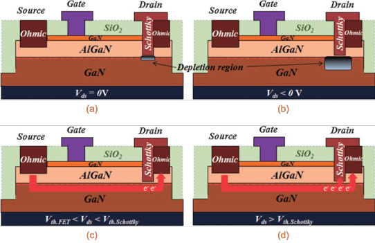
Figure 1: Operation mechanism of unidirectional AlGaN/GaN-on-Si HFET: (a) zero drain bias, (b) reverse drain bias, (c) small forward drain bias (less than Schottky turn-on voltage), and (d) large forward drain bias.
The Schottky recessing was achieved using buffer oxide etch for the silicon dioxide removal and inductively coupled plasma (ICP) reactive-ion etch (RIE) to drill into the nitride semiconductor layers. The Schottky contact of the drain electrode was deeply recessed 17nm into the AlGaN barrier “to achieve a low forward turn-on voltage while blocking the reverse current flow”. The researchers explain: “To block the reverse current flow, the recessed AlGaN barrier must be thin enough to completely deplete the 2DEG channel underneath.” The length of the Schottky contact was 3μm.
The gate-drain distance was 12μm, while the gate length was 3μm and the gate-source distance was 2μm. The device also included field-plates on the gate (2μm) and drain (1.5μm) contacts to further massage the electric fields so as to achieve high voltage breakdown performance.
The forward 1mA/mm turn-on voltage of the embedded Schottky diode was 0.4V. The forward voltage performance of the device is comparable with that of a conventional HFET without Schottky diode produced for comparison. While the conventional HFET was bidirectional, the embedded Schottky device limited reverse currents to less than 10-5A/mm (0.01mA/mm), indicating a completely depleted channel (Figure 2).
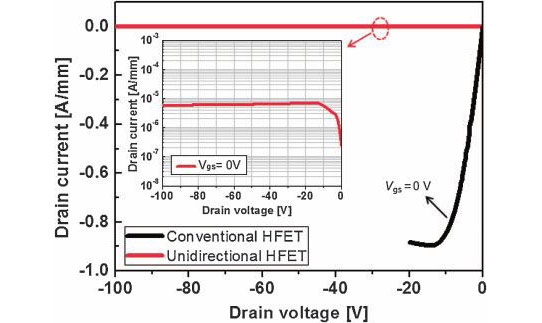
Figure 2: Comparison of reverse characteristics between conventional and unidirectional AlGaN/GaN-on-Si HFETs. Inset: reverse drain leakage current of unidirectional device under on-state (0V gate) condition.
The forward ‘off’ (gate potential -10V) and reverse ‘on’ (0V gate) catastrophic breakdown drain voltages for the unidirectional HFET were +615V and -685V, respectively. The conventional device suffered forward breakdown at +585V. The researchers believe the reduced breakdown in the conventional device can be mainly attributed to that device not having a drain field-plate, although it did have a gate field-plate.
The researchers carried out simulations in support of their belief. The need for the drain field-plate arises from the long gate-drain distance. In conventional AlGaN/GaN HFETs designed for RF operation rather than lower-frequency power switching, shorter gate-drain distances are used and then the field tends to peak near the gate rather than the drain. Also, if an optimum gate field-plate is employed to reduce the field peak near the gate edge, one has then to consider the peak near the drain edge to achieve further breakdown improvements.
http://dx.doi.org/10.7567/APEX.7.014101
The author Mike Cooke is a freelance technology journalist who has worked in the semiconductor and advanced technology sectors since 1997.


