


- News
25 June 2014
Techniques for high-efficiency nitride LEDs on lithium gallate substrate
South China University of Technology (SCUT) has produced m-plane indium gallium nitride (GaN) light-emitting diodes on lithium gallate (LiGaO2) (100) substrates [Wenliang Wang et al, Journal of Materials Chemistry C, vol2, p4112, 2014]. The researchers report that the best value of external quantum efficiency (EQE) of 50.8% is comparable to reported values of semi-polar GaN-based LEDs grown on bulk GaN substrate, and is much better than commercially available LED chips with EQEs of about 30%.
SCUT has worked for a while on growing non-polar m-plane nitride semiconductor layers on LiGaO2 [see e.g. PLD/MBE m-plane gallium nitride on lithium gallate]. It is hoped that production of GaN-based LEDs with the crystal layers oriented in the m-plane direction will boost efficiency through avoiding the electric fields that arise from the polarization of material grown in the usual c-plane direction. These electric fields inhibit recombination through the ‘quantum-confined Stark effect’ (QCSE) pulling the electrons and holes apart, severely reducing the ‘wavefunction overlap’.
Although non-polar and semi-polar bulk GaN and sapphire substrates are available, they are very expensive. A lower-cost option could be LiGaO2, although up to now there have been technological barriers to adoption. The SCUT team has developed new growth techniques to enable the development to go forward.
The m-plane heterostructure wafers (Figure 1) were produced by a combination of pulse laser deposition (PLD) and molecular beam epitaxy (MBE). The PLD was used to create a 50nm m-GaN buffer/nucleation layer on the bare substrate at 200°C. The use of low-temperature PLD and LiGaO2 avoids problems with thermal expansion and lattice mismatching in the early nucleation phase of the crystal growth, reducing the formation of threading dislocations. The low temperature also inhibits lithium diffusion from the substrate that has previously been a concern from the use of LiGaO2 substrates.
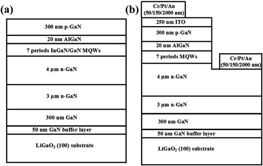
Figure 1: Schematic structures of (a) GaN-based LED wafer grown on LiGaO2(100) substrate, and (b) chip.
The temperature was then raised for the further layers grown by MBE at higher temperature: 500°C (300nm GaN), 750°C (3μm GaN, 4μm n-GaN), and 700°C for the multiple quantum well (MQW), AlGaN electron-blocking, and p-GaN contact layers.
The heterostructure material was fabricated into standard LED chips using inductively coupled plasma reactive-ion etch, 700°C thermal activation of the p-GaN, evaporation of indium tin oxide (ITO) as transparent conductive p-contact, deposition of n- and p-electrode metals, and a 1 minute 700°C anneal for ohmic contact formation. The wafers were finally singulated into 300μmx300μm LED chips.
Scanning-electron microscope (SEM) studies comparing the m-plane material with a similar structure grown on c-plane sapphire showed more pits and black spots in the latter material. The researchers comment: “We attribute these differences to the higher Mg-doping efficiency in non-polar m-plane p-GaN layers due to its higher hole concentration. The poorer Mg-doping efficiency in p-GaN grown on c-plane sapphire would introduce many more defects, such as pits and black spots.”
Hall measurements also showed improved electrical performance for the n-type and p-type regions (Table 1).
Table 1: Hall measurement results from van der Pauw configuration on n-GaN (silicon-doped) and p-GaN (magnesium-doped) layers.
| n-type mobility (cm2/V-s) | n-type carrier concentration | p-type mobility (cm2/V-s) | p-type carrier concentration | |
| m-GaN | 330 | 5.9x10¹⁸ | 12.5 | 2.8x10¹⁸ |
| c-GaN | 315 | 4.0x10¹⁸ | 9.5 | 4.9x10¹⁷ |
Atomic-force microscopy (AFM) gave a root-mean square (rms) roughness of 1.3nm for the m-plane structure, compared with 2.7nm for the c-plane material. Room-temperature photoluminescence also showed a stronger narrower peak for the m-plane InGaN/GaN MQWs at 446nm with full-width at half-maximum (FWHM) of 21.2nm, compared with 23.5nm for the c-plane structure.
The electroluminescence from the device blue-shifts slightly to shorter wavelengths as the current increases from 20mA to 150mA – an effect the researchers attribute to band filling where the average distance between the electron and hole states becomes wider at higher carrier concentrations, leading to higher-energy photons.
The FWHM of the spectral line remains fairly constant at ~20.5nm, in contrast to a c-plane comparison LED that has a width that increases from 21.25nm to 23.5nm over the 20mA to 150mA current range. The researchers ascribe the difference to the smaller lattice and thermal expansion contrast of the LiGaO2 substrate with m-plane GaN, compared with c-GaN on c-sapphire.
The light output power at 20mA was 30.1mW, compared with 19.2mW for the c-plane LED (Figure 2). The performance of the m-plane LED on LiGaO2 “is comparable to the best values ever reported for semi-polar or non-polar LEDs”, according to the team. The researchers add: “This great improvement in light output power is mainly attributed to the uniformity of current spreading in the LED chip on LiGaO2(100) due to the absence of the QCSEs in MQWs on LiGaO2 (100) substrate, which enhances the internal quantum efficiency (IQE) and external extraction efficiency.”
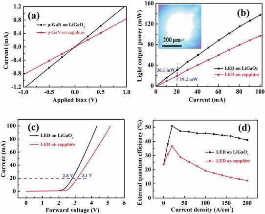
Figure 2: (a) Current–voltage characteristics of chromium/platinum/gold (Cr/Pt/Au) contacts on p-GaN grown on LiGaO2(100) and c-plane sapphire substrates, respectively, measured over Ohmic pads with spacing of 3mm. GaN-based LED chip characteristics: (b) light output power versus current (L–I), (c) current versus voltage (I–V), and (d) EQE versus current (EQE–I). Inset photograph: lit-up LED on LiGaO2(100) substrate at 20mA.
At the same current injection, the forward voltage is 2.8V, compared with 3.1V for the c-plane device. This indicates a reduction in series resistance from ~10Ω for the c-plane LED to ~7Ω.
Finally, the external quantum efficiency (EQE) of the m-plane LED remains relatively high at ~41% for a current injection density of 200A/cm2. By contrast, the c-plane LED shows a severe efficiency droop. The researchers attribute the high EQE for the m-plane device to the absence again of QCSE.
LEDs GaN Lithium gallate substrate MBE
http://dx.doi.org/10.1039/C4TC00192C
The author Mike Cooke is a freelance technology journalist who has worked in the semiconductor and advanced technology sectors since 1997.


