


- News
28 May 2014
GaN to grow at 9% CAGR to over 18% of RF device market by 2020
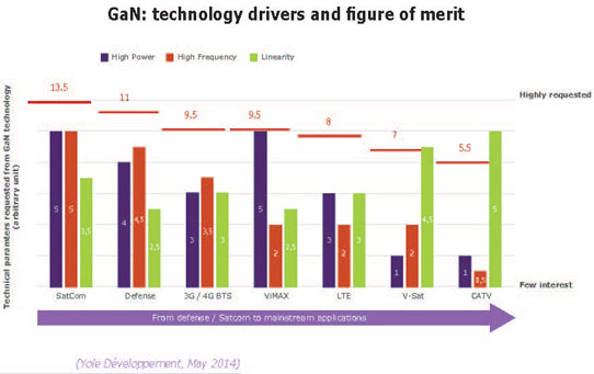
The need for high-power, high-frequency transistors is increasing steadily, commensurate with the huge demand for wireless telecommunications, notes market research firm Yole Développement in its report ‘RF GaN Technology & Market Analysis: Applications, Players, Devices & Substrates 2010-2020’. More power, more frequency bands, better linearity and improved efficiency are still driving the development of RF semiconductor devices, since the market needs devices able to handle all of these specifications at a reasonable price.
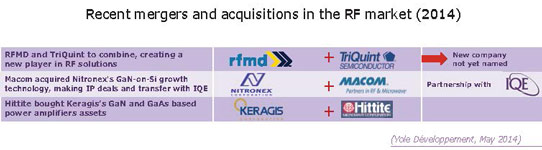
Recent mergers and acquisitions are a concern for the overall RF market and silicon LDMOS, gallium arsenide (GaAs) and gallium nitride (GaN)-based devices, says Yole. The overall RF market does not seem large enough for so many players, hence companies are trying to gain scale in order to increase profitability, which has stagnated. “We expect that commercial wireless telecom, CATV [cable television] and defense applications will be the main applications affected,” says Yole.
Although significant improvements have been achieved in RF GaN-based devices (performance and yields), Yole believes that there is still a barrier preventing gallium nitride on silicon carbide (GaN-on-SiC) from entering mainstream applications (i.e. in wireless telecom base-stations or CATV). In applications below 3.5GHz, GaN-on-SiC is not cost-effective enough versus Si-LDMOS, resulting in low market penetration rates, adds the firm. M/A-COM Technology Solutions Inc of Lowell, MA, USA and epiwafer foundry and substrate maker IQE plc of Cardiff, Wales, UK believe they will enter mass production using 6” and 8” GaN-on-Si substrates in two years. IQE will offer MACOM a significant mass-production level due to its existing production for other applications. “Our analysis shows that GaN-on-Si could be implemented in 2-5 years within telecom base-stations, MilCom [military communications] and CATV,” says Yole. “In this optimistic scenario, RF GaN-based devices could see an increased penetration rate and reach more than 20% of the overall RF device market by 2020,” it adds.
From defense to mainstream – RF GaN technology continues to be adopted for commercial applications
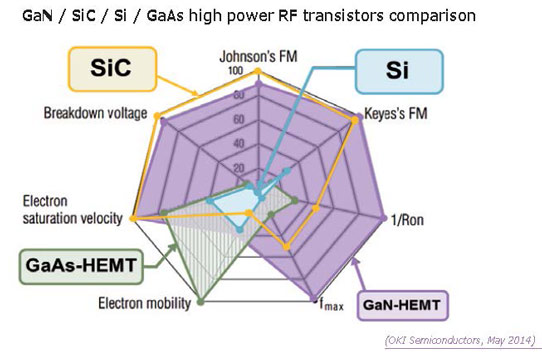
Over the last several years, silicon LDMOS’ share of high-power RF amplification applications in the 2GHz+ frequency range has fallen from 92% to 76%; the remaining 24% market share is addressed mainly by technologies such as GaAs pHEMT or GaN HEMTs. This equilibrium continues to be turned around by GaN HEMTs implementation, says Yole. The GaN HEMT in wireless telecoms is a higher-power and higher-frequency transistor alternative. From a system point of view, GaN is cost-competitive in applications over 3.5GHz. GaN devices continue to challenge the dominant position of silicon in an industrial playground in which a power amplifier (PA) market of $1600m+ is forecasted for 2020.
Today, several companies (i.e. Cree, Triquint/RF Micro Devices, Sumitomo, RFHIC, MACOM/Nitronex, Mitsubishi, NXP, Microsemi) have GaN device portfolios covering a wide range of applications. GaN has progressed significantly over the last five years; several thousand devices have been developed and implemented in applications such as radar, CATV, space applications with satellite communication, counter-IED jammers, CATV modules, 3G/4G base-stations, WIMAX/LTE PAs and general-purpose applications.
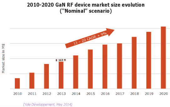
“In our nominal case, RF GaN-based devices could reach more than 18% of the overall RF device market by 2020 (i.e. a 9% CAGR [compound annual growth rate] from 2013-2020),” says Yole.
GaN devices offer added values over incumbent Si-LDMOS and GaAs HEMT
Yole notes that GaN offers better power capability and linearity compared with commonly used pure silicon or GaAs-based technologies, enabling higher performance and lower overall system costs, such as:
- higher efficiency (lower operating costs; improved module power density and size; and reduced cost of ownership);
- higher bandwidth and linearity (more versatile devices; fewer devices needed to cover the entire frequency spectrum; and cost savings at the development stage);
- higher polarization voltage (lower current level for the same power output; and fewer losses from the Joule effect, leading to cost savings in thermal management); and
- higher junction temperature (more robust devices, leading to improved expected lifetime and mean time to failure [MTTF]; and reduced cooling system demands, leading to cost savings at the system level [BTS]).
The report evaluates such added value, in addition to the production cost of GaN-based devices today and within 5 years. The production cost impact at the system level of the use of RF GaN devices is also analysed in detail, in order to understand the added costs at the device level and the cost savings at the system and module levels.
GaN-on-Si enabling GaN power electronics, but to capture less than 5% of LED making by 2020
www.i-micronews.com/reports/RF-GaN-Market-Analysis-Applications-Players-Devices/3/438


