


- News
21 October 2014
EVG introduces SmartNIL large-area nanoimprint lithography process
EV Group (EVG) of St Florian, Austria (a supplier of wafer bonding and lithography equipment for MEMS, nanotechnology and semiconductor applications) has introduced its SmartNIL large-area nanoimprint lithography (NIL) process. Available on all EVG NIL platforms, including mask aligners as well as the EVG720 and the new EVG7200 UV-NIL systems, SmartNIL provides a low-cost, large-area and high-volume manufacturing solution for a variety of advanced devices, including:
- photonic-based devices such as LEDs, lasers and photovoltaics;
- micro arrays and nano-devices for medical devices and bioengineered applications; and
- advanced storage media, including emerging forms of non-volatile memory (NVM).
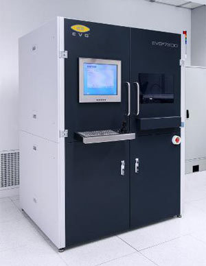 Picture: EVG’s SmartNIL large-area soft NIL process for high-volume manufacturing is available on the new EVG7200 automated UV-NIL system.
“SmartNIL is built on more than 15 years of NIL experience at EVG that includes the largest installed base of NIL systems worldwide, and is the only NIL technology currently used in high-volume manufacturing on substrates up to 200mm today,” says executive technology director Paul Lindner. “With our new EVG7200 UV-NIL system, which has industry-leading resolution down to 20nm in volume production, EVG brings the advanced soft stamp and imprint capability of SmartNIL to larger substrates and smaller geometries,” he adds. “This enables our customers to achieve even greater cost-of-ownership (CoO) benefits and realize the full manufacturing potential of nanoimprint lithography.”
The benefits of SmartNIL are said to include:
- Photonic devices (such as photovoltaics, LEDs, laser diodes and optical sensors) rely on the nano-scale manipulation of light to achieve optimal performance. This can be tailored by using nano-scale structures such as photonic crystals, gratings, phase-shift structures and wave guides.
- In bioengineered applications, nano-scale manufacturing processes are a requirement, since most biologic events begin at the nanometer scale.
- For both applications, traditional writing methods for producing nano-scale features either have extremely low throughput and hence cannot be easily scaled up for cost-efficient production (such as electron-beam writing) or have sufficient throughput but are too cost-prohibitive, such as stepper systems for optical lithography.
- Certain photonic and bioengineered applications can also realize greater throughput and CoO benefits from the ability to pattern 3D structures or different height levels in a single step, which can best be accomplished with a soft-stamp UV-NIL approach.
- SmartNIL coupled with the EVG720 system (for 150mm substrates), which is in use at multiple device manufacturers’ fabs, and the new EVG7200 system (for 200mm substrates) provides the optimal combination of high resolution, high alignment accuracy and high throughput in a cost-effective platform required for volume production for photonic and bioengineered device applications.
Key features of SmartNIL technology include the following:
- A large full-field imprint area (up to 200mm).
- The fastest full-substrate UV-NIL solution for high-volume-manufacturing applications (>40 substrates per hour for 200mm substrates).
- Integrated soft-stamp fabrication technology reduces tool footprint and provides fast replication (less than 10 minutes versus 24 hours or more with competing technologies).
- Enables patterning on highly topographical structures; less sensitive to bowed and warped wafers.
- Optimized releasing properties extend the lifetime of the stamp.
- Self-cleaning properties reduce particle contamination and improve overall processing yields.
- A room-temperature process avoids thermal mismatch and long-range structure distortion for improved alignment accuracy.
www.evgroup.com/en/products/lithography/nanoimprint_systems


