


- News
2 October 2014
Van der Waals epitaxy of GaN and blue LEDs
IBM T. J. Watson Research Center in the USA has developed a van der Waals epitaxial (vdWE) method for the growth of gallium nitride (GaN) on graphene that results in single-crystal quality comparable to growth on traditional substrates such as sapphire or silicon carbide (SiC) [Jeehwan Kim et al, Nature Communications, vol5, p4836, published 11 Sep 2014].
Further, the researchers demonstrated transfer of the crystal material to other materials, allowing re-use of the expensive graphene on SiC growth substrate. The team was able to reuse the substrate to create functioning blue light-emitting diodes (LEDs).
Although the lattice mismatch between graphene and GaN is around 23%, a number of research teams have been developing III-V semiconductor (e.g. GaN) growth on graphene. Graphene has strong in-plane bonds, but weaker vdW bonds between planes. It is hoped that the more relaxed vdW bonding will allow the formation of 3D crystals on the 2D graphene with larger lattice mismatches. However, there are challenges such as suppressed nucleation due to low adsorption and migration energies of adatoms leading to cluster growth rather than single-crystal films [see www.semiconductor-today.com/news_items/2014/SEP/UCLA_100914.shtml].
The IBM method starts by forming a graphene layer through graphitizing the surface of the SiC substrate. The graphene growth is self-limiting and results in a layer with vicinal steps that the researchers used as nucleation sites for the subsequent GaN epitaxy (Figure 1). The steps were 5-10nm high and the step terrace width was 5-10μm.
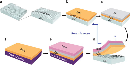
Figure 1: Schematic for growth/transfer of single-crystalline thin films on/from epitaxial graphene. (a) Graphitization of a SiC substrate to form epitaxial graphene. (b) Epitaxial growth of GaN on graphene. (c) Deposition of stressor layer (Ni). (d) Release of GaN from substrate with handling tape. (e) Transfer of released GaN/Ni/tape stack to host substrate. (f) Removal of tape and Ni by thermal release and wet etch, leaving GaN film.
A variety of metal-organic chemical vapor deposition (MOCVD) processes were tried to create GaN on graphene. The GaN epilayer was limited to an area of ~1cm2 due to the small MOCVD reactor that was used. The researchers found that a modified two-step process at 1100°C and 1250°C resulted in continuous and smooth GaN films.
This high-temperature two-step process contrasted with the usual low-temperature/high-temperature (580°C/1150°C) two-step process typically used for deposition on SiC or sapphire. In the case of GaN/graphene growth, the traditional two-step process resulted in GaN clusters. A one-step 1100°C growth resulted in stripes of GaN on graphene that was attributed to nucleation at the vicinal step edges. A one-step process at 1250°C resulted in no GaN growth due to the reduced sticking coefficient at higher temperature.
Electron microscope and diffraction analysis of the GaN film indicated planes of well aligned single-crystalline wurtzite. The researchers estimated the density of threading dislocations over a 30μm2 area at around 1x10⁹/cm2. “This density is in the comparable range with that of AlN-buffer-assisted GaN films grown on the conventional substrates, sapphire or SiC by using MOCVD (5x10⁸/cm2-8x109/cm2),” according to the team.
X-ray analysis gave a rocking curve full-width at half maximum (FWHM) value of 0.06° (216arcsec) for the (002) GaN peak. The researchers say this value is similar to that found for GaN on sapphire or SiC.
To release the GaN film, the researchers applied 2μm nickel as a stressor to create strain in the 2.5μm GaN film and release the GaN/graphene vdW bonds. Thermal release tape was applied to the nickel for handling and to allow transfer of the GaN layer to another host substrate. The release temperature of the tape was 90°C.
Atomic force microscopy (AFM) of the GaN surface that was attached to the graphene/SiC showed terrace structures. The researchers believe that this means the entire GaN layer was successfully removed from the growth substrate. Further, Raman spectroscopy could not detect any graphene residue on the released GaN film.
The low surface roughness of 5Å root mean square (rms) allowed the researchers to directly bond the GaN film to a 90nm silicon dioxide insulator layer on (001) silicon substrate. The researchers comment: “The transferred GaN on insulator shows perfect single-crystalline diffraction patterns, indicating no degradation of crystalline quality during the transfer process.”
The researchers contrast the low atomic-level surface roughness to the high roughness obtained using laser lift-off substrate separation. In particular, the atomic roughness allows direct bonding without the need for adhesive. Further, the reuse of the graphene/SiC growth substrate does not require post-release surface treatment before further MOCVD.
The graphene/SiC substrate was used repeatedly to grow GaN films, confirming the potential for the reuse of expensive SiC substrates. Iron chloride (FeCl3) solution was used to remove nickel residue from the previous release process.
The researchers grew an LED stack on a substrate that had previously been recycled three times. The stack consisted of three-period 3.5nm indium gallium nitride (InGaN) multiple quantum wells in GaN barriers, along with n- and p-type contact layers.
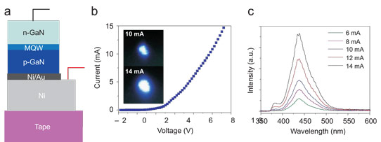
Figure 2: Fabrication of GaN blue LED transferred on tape. (a) Schematic of transferred visible LED device on tape. (b) Current versus voltage (I–V) characteristic of a transferred LED stack. Inset: pictures of LED emitting blue light. (c) Electroluminescence (EL) spectra of transferred LED stack.
Nickel/gold was applied to the top p-contact and the structure was released using the nickel stressor/thermal release tape technique. Direct electrical probing showed diode behavior and 440nm-wavelength blue electroluminescence (Figure 2).
Blue LEDs GaN GaN deposition on graphene Graphene MOCVD
http://dx.doi.org/10.1038/ncomms5836
The author Mike Cooke is a freelance technology journalist who has worked in the semiconductor and advanced technology sectors since 1997.


