


- News
17 September 2014
One-dimensional heterojunctions in metal dichalcogenide monolayers
Researchers based in the USA, UK, and Hong Kong have developed a physical vapor transport process that creates one-dimensional (1D) heterojunctions between metal dichalcogenide (MX2) two-dimensional (2D) semiconductor monolayers of molybdenum diselenide (MoSe2) and tungsten diselenide (WSe2) [Chunming Huang et al, Nat. Mater., published online 24 August 2014]. The team consisted of members from the University of Washington, University of Warwick, and University of Hong Kong.
MoSe2 and WSe2 have direct optical bandgaps of 1.550eV and 1.653eV, respectively. Direct bandgaps are needed for efficient optoelectronics. Further lattice constants of the two-dimensional materials are close to each other: 3.280Å for WSe2 and 3.288Å for MoSe2.
“Heterojunctions are fundamental elements of electronic and photonic devices,” comments Xiaodong Xu, an assistant professor of materials science and engineering and of physics at University of Washington. “Our experimental demonstration of such junctions between two-dimensional materials should enable new kinds of transistors, LEDs, nanolasers, and solar cells to be developed for highly integrated electronic and optical circuits within a single atomic plane.”
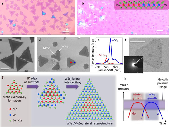
Figure 1: In-plane hetero-epitaxy of 2D MoSe2/WSe2 lateral heterostructures. a, Optical image of triangular heterostructure crystals. b, Optical image of semi-continuous film. Inset: side-view cartoon of in-plane heterojunction. c and d, SEM images of heterostructure crystals from two different growths. All scale bars 10μm. e, Raman spectra (514.5nm laser excitation) taken at points indicated in d. f, BF TEM image of isolated heterostructure. Inset shows electron diffraction pattern implying single undistorted lattice. Scale bar: 5μm. g, Schematic illustration of process of in-plane epitaxial growth of lateral heteostructures. h, Schematic of atomic vapor pressure variation leading to growth of two materials in sequence.
David Cobden, professor of physics at Univeristy of Washington adds: “In the future, combinations of two-dimensional materials may be integrated together in this way to form all kinds of interesting electronic structures such as in-plane quantum wells and quantum wires, superlattices, fully functioning transistors, and even complete electronic circuits.”
Recently, type II (staggered) band alignment (where excitons with electrons and holes are localized on opposite sides of the interface) has been suggested for vertical two-dimensional disulfide heterojunctions (MoS2/WeS2) [see the story ‘Ultrafast charge separation in metal dichalcogenide heterostructure’ on charge transfer in MoS2-WS2 at www.semiconductor-today.com/news_items/2014/SEP/UCB_160914.shtml]. The Washington/Warwick/Hong Kong team suggests that their horizontal MoSe2/WSe2 one-dimensional heterojunction may also lead to type II behavior, enabling efficient optoelectronics.
Growth of the lateral heterostructures was achieved through physical vapor transport from MoSe2 and WSe2 powders in hydrogen onto silica-on-silicon substrate in a one-inch tube furnace. The sources were heated to 950°C. The temperature in the substrate region of the tube was 650-750°C.
The researchers believe that a larger furnace would make it possible to mass-produce sheets of MoSe2/WSe2 semiconductor heterostructures. With the one-inch tube furnace, it took about five minutes to grow the crystals. However, the heating and cooling took up to two hours.
The growth process often resulted in monolayer crystal patches of approximately equilateral triangles of side 15μm. Other shapes were also seen: strips, stars, arrows... A wet process was used to transfer the monolayer material on poly(methyl methacrylate) (PMMA) to the analysis substrates (silicon dioxide, electron microscope grid, etc).
The triangular crystals tended to have darker inner regions and paler outer perimeters. Raman spectroscopy suggested that the inner regions tended to be MoSe2 and the outer regions WSe2. The researchers explain the structure as being due to MoSe2 growth being favored early on, but as the vapor pressure shifts, the growth tips towards crystal WSe2 monolayer coverage. The researchers add: “The similarity of the two materials permits the epitaxial growth of WSe2 directly on existing MoSe2 crystal edges.”
The shift in growth from MoSe2 to WSe2 may also be due to the different evaporation properties of the source powders.
The researchers comment: “The reproducibility of our results suggests that a more sophisticated setup with independent control of the vapor components could be developed if necessary to create heterojunction sequences programmably for complex device applications.”
Such sequences could be used to create one-dimensional quantum wells within the two-dimensional semiconductor monolayers.
Analysis with various techniques suggested that all the atoms lay on a single MX2 honeycomb lattice with no dislocations or grain boundaries. The interface between the MoSe2 and WSe2 regions occurs on a scale of several lattice constants. In the interface region the material is an alloy of the two materials – i.e. WxMo1-xSe2 with a steep x-composition gradient from 0 to 1. Away from the interface the researchers found some Mo substitutions on the WSe2 side. Also, some Se vacancies were apparent.
Microscopic photoluminescence (PL) studies showed exciton peaks at 1.57eV and 1.63eV in the MoSe2 and WSe2 regions, respectively (Figure 2). These are “identical” with the values found for homogeneous MoSe2 and WSe2 monolayers.
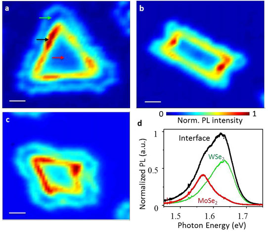
Figure 2: Photoluminescence from 1D heterointerfaces. a, 2D PL intensity map of triangular lateral heterostructure. Scanning micro-PL was performed with 532nm laser excitation at room temperature. b and c, Similar measurements for heterostructures with other shapes. Scale bars: 2μm. d, PL spectra taken at points indicated in a.
The peak for the heterojunction region was intermediate in energy and broader than for the pure MoSe2/WSe2 regions. Also, the emission was brighter – “possibly due to trapping of excitons by defects or enhanced radiative recombination at the interface”.
As yet, no electron transport study has been made due to the lack of a suitable, reliable contact structure.
Transistors LEDs Nanolasers Solar cells
http://dx.doi.org/10.1038/nmat4064
The author Mike Cooke is a freelance technology journalist who has worked in the semiconductor and advanced technology sectors since 1997.


