


- News
17 June 2016
Speed up for indium gallium nitride two-dimensional electron gas
Xidian University in China has used pulsed metal-organic chemical vapor deposition (MOCVD) to increase indium gallium nitride (InGaN) room-temperature channel mobility to 1681cm2/V-s, which is claimed to be a record [Yachao Zhang et al, Appl. Phys. Express, vol9, p061003, 2016]. The team comments: "The results in this paper demonstrate the superiority of the InGaN channel heterostructure over the conventional GaN channel heterostructure, especially at elevated temperature, indicating its huge potential in high-power and high-frequency applications."
Xidian has used pulsed MOCVD for some time to achieve improved III-nitride quality for aluminium nitride (AlN) and InGaN [e.g. www.semiconductor-today.com/news_items/2015/aug/xidian_130815.shtml, http://dx.doi.org/10.1063/1.4937127]. In pulsed MOCVD, the precursor sources of the elements are supplied in particular sequences. InGaN growth proceeds by depositing a sequence of short-period GaN and InN layers as a superlattice. "This change in the growth mode increases the surface mobility of adatoms and enables them to find energetically favorable locations," the researchers explain.
The researchers see the applications for InGaN high-mobility channels as being higher-speed and higher-frequency microwave power devices. The narrower bandgap of InGaN should reduce the effective mass, increasing carrier speeds for a given electric field. The (slight?) penalty would be a somewhat reduced critical field, reducing breakdown voltages. In fact, mobilities higher than GaN channels have not been achieved as yet.
Until the latest Xidian work, the best reported figure the team points to was 1295cm2/V-s. The problems seem to revolve around alloy disorder and interface roughness. Both these factors increase carrier scattering, which in turn reduce mobility and increase sheet resistance.
Another advantage of InGaN is increased confinement of the two-dimensional electron gas (2DEG) channel with a top and bottom barrier structure. The team comments: "Previous reports have shown that devices with an InGaN channel exhibit excellent performance by some measures, such as suppression of current collapse and the virtual gate effect."
The heterostructure (Figure 1) was grown on (0001) sapphire using a home-made vertical low-pressure MOCVD system. The metal-organic sources were trimethyl-aluminium, -gallium, and -indium. The nitrogen source was ammonia. The GaN buffer and AlGaN barrier were grown at 940°C. The pulsed part of the process, creating the InGaN layer, was carried out at 740°C.
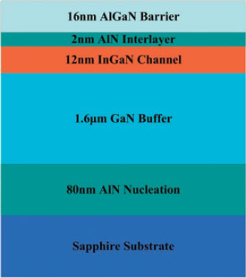 Figure 1: Schematic cross-section of AlGaN/InGaN heterostructure.
The 2nm AlN interlayer was formed by a two-step process. This interlayer was designed to improve interface morphology between the InGaN channel and barrier and to protect the high-quality InGaN channel from damage during the subsequent high-temperature growth.
X-ray analysis suggested that the AlGaN alloy barrier had a 35% AlN mole fraction, according to Vegard's law. The x-ray signal for the InGaN layer was much stronger than for previous work, indicating the high quality of the pulsed MOCVD process. The InN mole fraction was estimated at 5%. Photoluminescence experiments also gave 5% for the InN content of the InGaN layer.
Secondary-ion mass spectrometry (SIMS) on samples with and without an interlayer showed that the 2nm AlN effectively prevented indium atom losses during growth of the high-temperature AlGaN barrier.
Atomic force microscopy (AFM) on a sample without the AlGaN barrier layer gave a root-mean-square (rms) roughness of 0.19nm over a 2μmx2μm field. With the AlGaN barrier, the roughness was 0.15nm. The researchers comment: "The result is even better than that obtained for conventional AlGaN/GaN heterostructures, proving that there is negligible structural degradation in the AlGaN barrier when it is grown on the InGaN channel."
Temperature-dependent Hall measurements show the InGaN channel to have lower mobility than pure GaN up to 360K (Figure 2, room temperature ~300K). Beyond that, the InGaN channel has the edge. "These results demonstrate the superiority of the InGaN-channel heterostructure over the conventional GaN-channel heterostructure for fabricating high-power and high-frequency devices, which often operate at elevated temperature in practical applications," the researchers write.

Figure 2: Temperature dependence of 2DEG mobility (μ) and sheet resistance (Rs) for InGaN-channel and GaN-channel heterostructures. Inset carrier density (ns) as a function of temperature.
At the same time, the carrier density in the InGaN two-dimensional electron gas (2DEG) channel is higher than for GaN – 1.3x10¹³/cm2 versus 0.9x10¹³/cm2, respectively – giving a lower overall sheet resistance. The researchers attribute the higher carrier density to improved 2DEG confinement. The team believes that the 1.3x10¹³/cm2 density can be improved by increasing the AlGaN barrier thickness or the AlN mole fraction.
Comparing with previous work, the researchers comment: "A record highest room-temperature electron mobility of 1681cm2/V-s is obtained in our experiment, which is far superior to the other reported results."
The team attributes the performance to improved InGaN crystal quality from pulsed MOCVD growth and the use of the AlN interlayer to suppress alloy disorder and interface roughness.
Indium gallium nitride two-dimensional electron gas MOCVD
http://dx.doi.org/10.7567/APEX.9.061003
The author Mike Cooke is a freelance technology journalist who has worked in the semiconductor and advanced technology sectors since 1997.


