


- News
14 June 2017
Imec develops 200V and 650V dispersion-free normally-off/E-mode power devices on 200mm silicon
Nanoelectronics and photovoltaics research centre Imec of Leuven, Belgium has developed 200V and 650V normally-off/enhancement mode (E-mode) on 200mm/8-inch gallium nitride on silicon (GaN-on-Si) wafers, achieving a very low dynamic Ron dispersion (below 20%) and what is claimed to be state-of-the-art performance and reproducibility. Stress tests have also shown good device reliability, it adds. Imec’s technology is ready for prototyping, customized low-volume production and technology transfer.
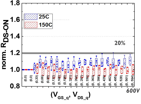
Picture: Dynamic RDS-ON dispersion (10µs on – 90µs off) of Imec’s 650V GaN-on-Si E-mode device technology measured at 25°C and 150°C.
GaN technology offers faster-switching power devices with higher breakdown voltage and lower on-resistance than silicon, making it a suitable material for advanced power electronic components. Imec says that its GaN-on-Si device technology is gold (Au)-free and compatible with the wafer handling and contamination requirements for processing in a silicon fabrication plant.
A key component of the GaN device structure is the buffer layer, which is required to accommodate the large difference in lattice parameters and thermal expansion coefficient between the AlGaN/GaN materials system and the silicon substrate. Imec has developed a patent pending buffer design that allows growth of buffers qualified for 650V on large-diameter 200mm wafers. This, in combination with the choice of the silicon substrate thickness and doping, increased the GaN substrate yield on 200mm to competitive levels, enabling low-cost production of GaN power devices, says Imec.
In addition, the cleaning and dielectric deposition conditions have been optimized, and the field-plate design (a common technique for achieving performance improvement) has been studied extensively. As a result, the devices exhibit dynamic Ron dispersion below 20% up to 650V over the full temperature range of 25-150°C. This means that there is almost no change in the transistor on-state after switching from the off-state (a challenge typical for GaN technology).
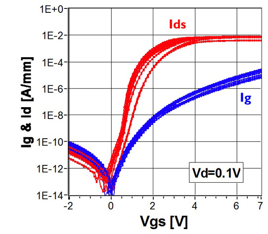
Picture: Transfer characteristic of 36mm-gate-width imec’s 650V GaN-on-Si e-mode transistors.
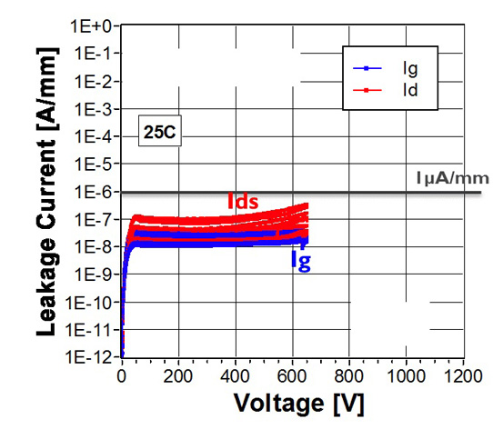
Picture: Leakage characteristic at VGS=0V of 36mm gate width imec’s 650V GaN-on-Si e-mode transistors.
“Having pioneered the development of GaN-on-Si power device technology on large-diameter substrates (200mm/8-inch), Imec now offers companies access to its normally-off/e-mode GaN power device technology through prototyping, low-volume manufacturing as well as via a full technology transfer,” says Stefaan Decoutere, Imec’s program director for GaN technology. “Next to enhancement-mode power device switches, Imec also provides lateral Schottky diodes for power switching applications,” he adds. “Based on Imec’s proprietary device architecture, the diode combines low turn-on voltage with low leakage current, up to 650V – a combination that is very challenging to achieve.”
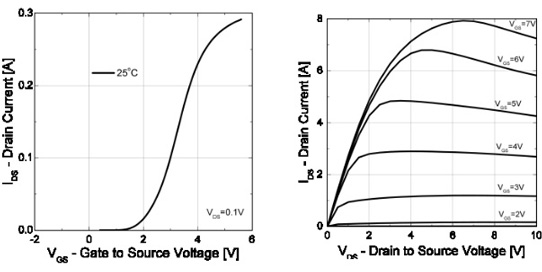
Picture: Typical output characteristic and transfer characteristic of 36mm-gate-width 650V GaN-on-Si e-mode device technology.
Imec extends GaN-on-Si R&D initiative for joint research on 200mm epi and E-mode device


