


- News
20 September 2017
HKUST/UCSB team demonstrates record 1.3μm CW submilliamp-threshold quantum dot micro-lasers on silicon
With the increasing need for miniaturization and large-scale integration of photonic components on a silicon platform for datacoms and emerging applications in mind, a team of researchers at the Hong Kong University of Science and Technology (HKUST) and the USA’s University of California, Santa Barbara (UCSB) have demonstrated record-small electrically pumped micro-lasers epitaxially grown on industry standard (001) silicon substrates (Yating Wan et al, ‘1.3μm submilliamp threshold quantum dot micro-lasers on Si’, Optica vol4, issue 8, p940 (2017)). A submilliamp threshold of 0.6mA, emitting continuous-wave (CW) at the near-infrared telecommunications wavelength of 1.3μm up to 100°C, was achieved for a micro-laser with a radius of 5μm. The thresholds and footprints are orders of magnitude smaller than those previously reported lasers epitaxially grown on silicon.
“We demonstrated the smallest-current-injection QD lasers directly grown on industry-standard (001) silicon with low power consumption and high temperature stability,” says Kei May Lau, Fang Professor of Engineering and Chair Professor in HKUST’s Department of Electronic & Computer Engineering. “The realization of high-performance micron-sized lasers directly grown on silicon represents a major step toward utilization of direct III-V/Si epitaxy as an alternate option to wafer-bonding techniques as on-chip silicon light sources with dense integration and low power consumption,” he adds.
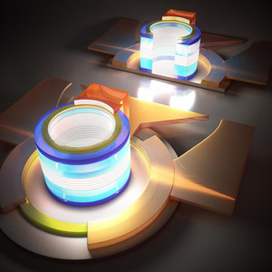 Picture: Schematic of electrically pumped quantum dot micro-ring laser. (Credit: Department of Electronic and Computer Engineering, HKUST.)
The two groups have been collaborating and have previously developed CW optically pumped micro-lasers operating at room temperature that were epitaxially grown on silicon with no germanium buffer layer or substrate miscut. This time, they demonstrated record-small electrically pumped QD lasers epitaxially grown on silicon. “Electrical injection of micro-lasers is a much more challenging and daunting task: first, electrode metallization is limited by the micro-size cavity, which may increase the device resistance and thermal impedance; second, the whispering gallery mode (WGM) is sensitive to any process imperfection, which may increase the optical loss,” notes Yating Wan, a HKUST PhD graduate and now postdoctoral fellow in UCSB’s the Optoelectronics Research Group.
“As a promising integration platform, silicon photonics need on-chip laser sources that dramatically improve capability, while trimming size and power dissipation in a cost-effective way for volume manufacturability,” comments John Bowers, deputy CEO of AIM Photonics. “The realization of high-performance micron-sized lasers directly grown on silicon represents a major step toward utilization of direct III-V/Si epitaxy as an alternate option to wafer-bonding techniques.”
Subwavelength micro-disk lasers on exact (001) silicon substrate
HKUST Direct epitaxy of III-V quantum dot materials on silicon Microdisk lasers
https://doi.org/10.1364/OPTICA.4.000940
http://optoelectronics.ece.ucsb.edu/profile/john-bowers


