


- News
19 December 2019
Monolithic optoelectronic integration of gallium nitride transistor
Nanjing University of Posts and Telecommunications in China claims the first enhancement-mode metal-oxide-semiconductor field-effect transistors (MOSFETs) fabricated on a gallium nitride (GaN)-on-silicon light-emitting diode (LED) epitaxial wafer [Jiabin Yan et al, IEEE Electron Device Letters, published online 11 November 2019]. Enhancement-mode devices (that are ‘normally-off’ at 0V gate potential) are often preferred with respect to lower power consumption.
The research team also demonstrated the MOSFET’s ability to control an indium gallium nitride (InGaN) LED on the same platform. The researchers hope that such monolithic optical electronic integrated circuits (OEICs) could lead to applications such as smart lighting, display, and visible light communication (VLC). The Nanjing group has been developing VLC systems on silicon for a while [see e.g. www.semiconductor-today.com/news_items/2019/jun/nupt-130619.shtml, which contains further links].
The team sees advan tages to the low-cost silicon platform as including integration with micro-electro-mechanical system (MEMS) batch fabrication processes. Although LEDs, photodiodes, waveguides, couplers and other photonic structures are relatively easy to process, up to now GaN transistor structures are usually implemented using different epitaxial structures, impeding low-cost integration.
The III-nitride structure on silicon (Figure 1) included a 250nm InGaN/GaN multiple quantum well (MQW) layer sandwiched between n- and p-type GaN, as used in light-emitting diodes. The wafer was 2-inches in diameter. The silicon substrate was thinned to 300μm thick by grinding and polishing.
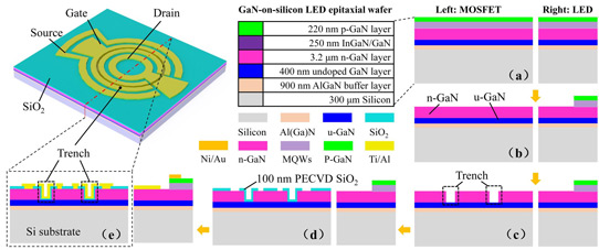
Figure 1: Schematic overview of proposed devices based on GaN-on-silicon platform and fabrication process steps.
The transistor was formed using the n-GaN as source and drain, while the channel was through the undoped GaN layer. Insulation and the gate dielectric consisted of 100nm silicon dioxide (SIO2). The gate metal was deposited in the trenches, covering the undoped GaN channel and the recess sidewalls. The electrodes were ring-shaped to increase the width/length ratio for a larger output current. The channel length was 20μm. The radius of the recess ring center was 135μm.
The fabrication began with removal of the p-GaN and InGaN/GaN layers using inductively coupled plasma reactive-ion etch from the transistor area. The gate recess also used a similar etch process, but at slow speed to ensure accurate depth with full removal of the n-GaN and non-removal of undoped GaN. Despite the slow etch, the sidewalls of the recess were rough.
The SiO2 was applied using plasma-enhanced chemical vapor deposition (PECVD) and patterned with reactive-ion etch. The transistor metals were titanium/aluminium, annealed to improve the source/drain ohmic contacts.
In DC testing the minimum on-resistance of 5Ω-m was achieved at 12V gate potential. The team comments: “Even though the output current is relatively low compared with that of some published GaN-based FETs, the proposed MOSFET can still meet the requirements of numerous low-power applications, especially the micro-LED for smart display (typical driving current from several μA to hundreds of μA).”
The subthreshold behavior was pretty poor with 2.78V/decade swing at 1V drain bias. This must be seen in the context that the theoretical minimum is 60mV/decade (0.06V/decade) at room temperature. Further, other reported GaN MOSFETs have achieved values as low as 218mV/decade. The researchers hope to improve the subthreshold behavior with tetramethylammonium hydroxide (TMAH) or fluorine treatments to reduce surface roughness of the recess sidewalls.
By contrast, the threshold voltage was a high 6.01V. The peak transconductance was 3.78μS/mm with the on-resistance at 7.96Ω-m. The drain bias was 0.1V. The gate and drain leakage currents were 120nA/mm (0V drain, 12V gate) and 5μA/mm (5V drain, 0V gate), respectively. An analysis of the parasitic capacitance suggests a cut-off frequency of the order of tens of megahertz. Reduced device dimensions would increase switching speed at the expense of drive current.
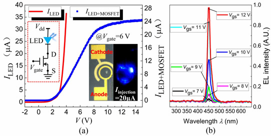
Figure 2: (a) Current-voltage (IV) characteristics of individual LED and LED-MOSFET (LED and MOSFET in series according to inset circuit diagram); (b) electroluminescence (EL) spectra of LED with different MOSFET gate voltages.
The researchers also integrated the MOSFET with an LED on the same substrate. The LED used titanium/aluminium and nickel/gold as cathode and anode electrodes, respectively. The MOSFET allowed control of the light output with increased gate potential (Figure 2).
https://doi.org/10.1109/LED.2019.29529058
The author Mike Cooke is a freelance technology journalist who has worked in the semiconductor and advanced technology sectors since 1997.


