


- News
13 June 2019
Developing III-nitride-on-silicon optoelectronic platform
China’s Nanjing University of Posts and Telecommunications continues to develop III-nitride optoelectronic systems with light-emitting diodes (LEDs) and photodiodes (PDs) connected with waveguides [Yongjin Wang et al, Semicond. Sci. Technol., vol34, 065017, 2019]. The new work used a metal-bonded III-nitride-on-silicon platform “for the first time”, according to the researchers.
The platform was also used in the group’s recent work on enhancing LED extraction by eliminating waveguide modes in the LED itself by the thinning of epitaxial layers [www.semiconductor-today.com/news_items/2019/mar/nupt_190319.shtml]. Previously, the Nanjing researchers constructed LED/PD systems that were transferred to glass [www.semiconductor-today.com/news_items/2018/may/nagoya_020518.shtml].
In the latest work, III-nitride thin-film material was metal-bonded to (100) silicon. The film was flipped so that the 125nm p-GaN side was down. The other layers consisted of a 50nm multiple quantum well, a 70nm InGaN spacer, and a 2800nm top n-GaN contact. On top of the n-GaN there was also 800nm undoped GaN and 700nm from the AlN/AlGaN buffer layers from the epitaxial growth process. The metal bonding included a silver reflector.
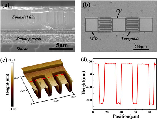
Figure 1: (a) Cross-sectional scanning electron microscope (SEM) image of III-nitride films on Si (100) substrate. (b) SEM image of on-chip power monitoring system. (c) Three-dimensional atomic force microscope image of waveguides. (d) Device height profile.
The device structure (Figure 1) was created using mesa and waveguide etching down to the silver-bonding layer, isolating the components electrically. The etch plasma consisted of a mix of chlorine and boron trichloride gases. Further patterned etching defined the p- and n-contact areas. Contact electrodes consisted of nickel/gold.
The device incorporated two LEDs and a central photodiode. The different sections were connected with waveguides consisting of 155μm-long fingers. The width and height of the waveguides were 18μm and 1253nm, respectively.
The light from the LEDs was transmitted along the waveguides and then across a 12μm air gap into the photodiode. The researchers see such structures as having potential for liquid and gas analysis, where fluids would flow through isolation trenches and channels, modulating light propagation.
The LED emission peak was at ~452nm, which was in the range of detection of the photodiode. By imposing different signals on the left and right LEDs, the researchers were able to distinguish the responses in the superposed photodiode output signal (Figure 2).
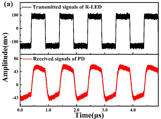
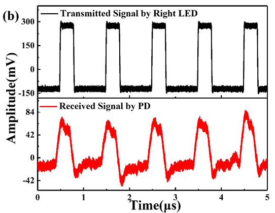
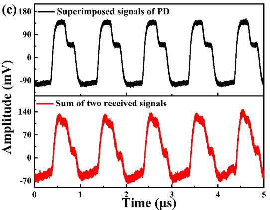
Figure 2: Transmitted signals of LEDs versus induced photocurrent temporal traces of photodiode: (a) R-LED and (b) L-LED. (c) Measured superimposed signals versus calculated signals.
The filling factor of the right LED was found to be 0.5 under 1MHz pulses with 0.4V peak-to-peak voltage and 5.0V offset. The left LED had a filling factor of 0.3. The researchers comment: “The filling factor of signals constitutes the codes used by the LEDs to modulate light for information transfer in the system.”
The team adds: “If the received signals from one LED is measured, the received signals from another LED can be obtained by subtracting the known signals using the superimposed signals. According to the difference in the filling factor, the mixed signals can be extracted to identify the individual LED.”
The researchers see the system being used as an on-chip monitor, enabling one photodiode to check dynamic emission power fluctuations from multiple LEDs.
Reflectivity studies suggested that thinning the epitaxial layer - confining the Fabry-Perot modes of the waveguide - could enhance light extraction in the systems.
LEDs GaN Photodiodes Waveguides
https://doi.org/10.1088/1361-6641/ab1d42
The author Mike Cooke is a freelance technology journalist who has worked in the semiconductor and advanced technology sectors since 1997.


