


- News
9 July 2019
Ascatron secures €3.5m funding for 3DSiC product development
Ascatron AB of Kista, Stockholm, Sweden (which was spun out of research institute Acreo in 2011) recently completed the sale of shares in a joint venture company in China, hence securing €3.5m funding to continue the independent development of its own products.
Ascatron develops silicon carbide (SiC) power semiconductors using its proprietary 3DSiC technology. The firm focuses on supplying bare SiC dies for power modules and discrete components.
The business model is semi-fabless, where Ascatron designs the power device and maintains in-house production of the key epitaxy material (with development and material production in Stockholm), while chip fabrication is outsourced (with the fabrication process for volume production of SiC power diodes and MOSFETs established at an automotive-qualified SiC foundry).
In addition to the general advantages of SiC, Ascatron says that its 3DSiC technology enables up to 30% lower power dissipation, higher current density and improved reliability.
“We use advanced epitaxial growth as part of the manufacturing process of our SiC devices to form buried doped structures as voltage-blocking elements,” says chief technology officer Adolf Schöner. “These structures protect the sensitive die surface from high electric fields and allow device designs optimized for high power ratings,” he adds. “The key performance advantages are 15-30% higher current density and reliable operation even at elevated temperatures”.
The first 3DSiC devices available for design-in projects with customers are 1200V and 1700V junction-barrier Schottky (JBS) diodes. The production process is expected to be qualified in fourth-quarter 2019. The design is modular and can be tailored to application-specific requirements. MOSFETs will be ready for production in second-quarter 2020.
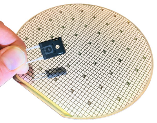
Picture: A 150mm device wafer with Ascatron 3DSiC JBS diodes rated for 1700V and 20A.
“The cost advantage of our 3DSiC devices comes into play especially at higher voltage and current ratings,” says CEO Christian Vieider. “The near-term target for our SiC diodes are 1200V and 1700V power modules. Next step will be to scale-up our SiC device wafer capacity together with our production partners.”
Ascatron produces its SiC epitaxy material with what it clains to be state-of-the-art thickness and doping homogeneity also for thick layers, enabling a high manufacturing yield for devices with high voltage and high current ratings. The firm will continue to provide its industry-proven SiC epitaxy services to customers.
Ascatron launches its first SiC power device products
Ascatron raises €4m in A-round funding for final development of its first SiC products
Ascatron and LPE cooperate on 150mm SiC epitaxy for power electronics
Quadrivio and Como Venture take 16.7% stake in Ascatron as part of A-round fundraising
Norstel and Ascatron ally to provide complete SiC epi offering
Ascatron spun off from Sweden's Acreo as first independent pure-play SiC foundry
SiC epitaxy SiC devices Power electronics


