
| Home | About Us | Contribute | Bookstore | Advertising | Subscribe for Free NOW! |
| News Archive | Features | Events | Recruitment | Directory |
CMP PROCESSING
Learn more about R&D chemical mechanical polishing by requesting our FREE informational CD.

| FREE subscription |
| Subscribe for free to receive each issue of Semiconductor Today magazine and weekly news brief. |
News
2 November 2007
Micromem’s GaAs MRAM device processed at GCS
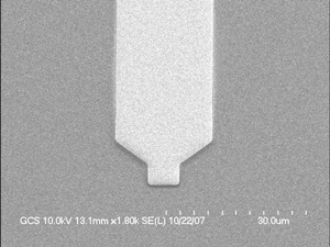
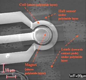
Micromem Technologies Inc of Toronto, Canada says that the GaAs wafer foundry Global Communication Semiconductors Inc (GCS) of Torrance, CA, USA has successfully patterned and processed the magnetic yoke design for its magnetic random access memory (MRAM).
Micromem’s prototype MRAM devices entered production at GCS on 20 September after its design partner, engineering company Strategic Solutions of Grass Valley, CA, USA (which Micromem contracted to design and implement the MRAM technology) released the approved reticle design to the foundry.
The production-level process yielded an extremely clean magnetic storage element while, at the same time, opening up the path towards memory size reductions and lower cost-per-bit.
Micromem says that the process of establishing the function and scalability of the multi-bit MRAM has followed a sequence of first productizing the magnetic storage element (the yoke), followed by Hall cross-sensor characterization, and finally integrated MRAM bit cell performance. With this successful demonstration of the magnetic structure, Strategic Solutions has characterized the relative efficacy of two alternative methods, electroplating versus sputter deposition, as they relate to the ultimate manufacturing of an MRAM product in a dense multi-bit array.
Similar data for Hall cross sensors should be seen in November. Micromem expects a demonstration of a fully integrated MRAM storage cell by year end.
Micromem says that it is in discussions with a major military-focused company that provides GaAs space-based platforms, centered around the proposed MRAM architecture and how it will benefit their current product line in a dense memory array format. “Now that we have structures coming out of the foundry that are showing scalability and that confirm the University of Toronto prototype and ongoing simulation modeling, it is invaluable to have the input from users,” says Steven Van Fleet, program director for the foundry phase of the commercialization process. “Our goal is to incorporate their insight as we move forward not only in deciding upon the initial memory array size they require but also by what process they will want the memory manufactured,” he adds. “Our plan is to engage such companies in a cross-licensing procedure. Now that structures are being validated in the foundry we can pursue these discussions in earnest."
Jon Scadden of Strategic Solutions says he is encouraged by the ultimate simplicity of Micromem’s MRAM design. “It predicts robust product performance and extremely good reliability and radiation-hardness,” he adds. “It enables an excellent match up to the knowledge base and skill sets of our foundry partner, GCS.”
See related items:
Micromem engages GCS as foundry for MEMS
GCS and RFIC Solutions ally on design services
Search: GCS
Visit: www.micromeminc.com
Visit: www.gcsincorp.com![]()
![]() ©2007 Juno Publishing and Media Solutions Ltd. All rights reserved. Semiconductor Today and the editorial material contained within it and related media is the copyright of Juno Publishing and Media Solutions Ltd. Reproduction in whole or part without permission from Juno Publishing and Media Solutions Ltd is forbidden. In most cases, permission will be granted, if the author, magazine and publisher are acknowledged.
©2007 Juno Publishing and Media Solutions Ltd. All rights reserved. Semiconductor Today and the editorial material contained within it and related media is the copyright of Juno Publishing and Media Solutions Ltd. Reproduction in whole or part without permission from Juno Publishing and Media Solutions Ltd is forbidden. In most cases, permission will be granted, if the author, magazine and publisher are acknowledged.
Disclaimer: Material published within Semiconductor Today and related media does not necessarily reflect the views of the publisher or staff. Juno Publishing and Media Solutions Ltd and its staff accept no responsibility for opinions expressed, editorial errors and damage/injury to property or persons as a result of material published.
Semiconductor Today, Juno Publishing and Media Solutions Ltd, Suite no. 133, 20 Winchcombe Street, Cheltenham, GL52 2LY, UK
Web site by No Name No Slogan ![]()