| Home | About Us | Contribute | Bookstore | Advertising | Subscribe for Free NOW! |
| News Archive | Features | Events | Recruitment | Directory |
| FREE subscription |
| Subscribe for free to receive each issue of Semiconductor Today magazine and weekly news brief. |
News
17 March 2009
JPSA introduces dual side scribe (DSS) capability for laser systems
At this week’s SEMICON Shanghai 2009 event in China, JP Sercel Associates Inc (JPSA) of Manchester, NH, USA is introducing new dual side scribe (DSS) processing capability on its laser wafer scribing systems, for performing both front-side and back-side scribing for LED, sapphire, gallium arsenide (GaAs), silicon, and metal wafers (depending on wafer processing requirements).
 JPSA’s proprietary back-side camera technology provides high accuracy with fast alignment times for the DSS systems. The firm has achieved high-throughput back-side scribing at speeds of up to 150mm per second with no debris or damage to the epitaxial layer.
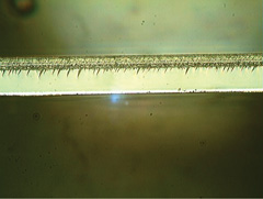
Picture: LED backside scribing: a 30 micron deep scribe in sapphire at 130mm/s, showing the unaffected epi-layer.
The DSS capability is also available as a field upgrade to all existing JPSA scribing systems, such as the IX 210, IX 300 and IX 6100. DSS also allows for easy conversion from front-side to back-side scribing.
“For many years, JPSA has been at the forefront of advanced deep UV front-side laser scribing,” claims president Charlie Cuneo. “With our recent advances in back-side scribing, namely a new laser absorption enhancement technique, we are able to offer our customers their choice of highly efficient scribing processes that best meets their production requirements,” he adds.
See related items:
JPSA ships laser-based LED lift-off system to FOREPI
![]() Search: JPSA LEDs Wafer scribing GaAs Sapphire
Search: JPSA LEDs Wafer scribing GaAs Sapphire
Visit: www.jpsalaser.com

![]() ©2009 Juno Publishing and Media Solutions Ltd. All rights reserved. Semiconductor Today and the editorial material contained within it and related media is the copyright of Juno Publishing and Media Solutions Ltd. Reproduction in whole or part without permission from Juno Publishing and Media Solutions Ltd is forbidden. In most cases, permission will be granted, if the author, magazine and publisher are acknowledged.
©2009 Juno Publishing and Media Solutions Ltd. All rights reserved. Semiconductor Today and the editorial material contained within it and related media is the copyright of Juno Publishing and Media Solutions Ltd. Reproduction in whole or part without permission from Juno Publishing and Media Solutions Ltd is forbidden. In most cases, permission will be granted, if the author, magazine and publisher are acknowledged.
Disclaimer: Material published within Semiconductor Today and related media does not necessarily reflect the views of the publisher or staff. Juno Publishing and Media Solutions Ltd and its staff accept no responsibility for opinions expressed, editorial errors and damage/injury to property or persons as a result of material published.
Semiconductor Today, Juno Publishing and Media Solutions Ltd, Suite no. 133, 20 Winchcombe Street, Cheltenham, GL52 2LY, UK
Web site by No Name No Slogan ![]()