| Home | About Us | Contribute | Bookstore | Advertising | Subscribe for Free NOW! |
| News Archive | Features | Events | Recruitment | Directory |
News
15 April 2010
Good grades for GaN HEMT ohmic source/drain contacts
University of California Santa Barbara (UCSB) researchers have used graded indium gallium nitride (InGaN) layers to create an ‘ultra-low’ contact resistance ohmic contacts for nitride high-electron-mobility transistors (HEMTs) with a non-alloy metal [Sansaptak Dasgupta et al, Appl. Phys. Lett., vol96, p143504, 2010]. The researchers achieved contract resistances as low as 27Ω-μm.
Nitride semiconductor HEMTs using aluminum gallium nitride/gallium nitride (AlGaN/GaN) layers to create high-mobility two-dimensional electron gas (2DEG) channels are of interest for high-power radio-frequency power amplification, but the performance with small signals is limited at present because of parasitic resistance, a substantial part of which arises in the source/drain ohmic contacts. These parasitic resistances lower the obtained cut-off (fT) and maximum oscillation (fmax) frequency performance.
The researchers used polarization effects of the nitride semiconductor to create ‘three-dimensional electron gases’ in the source/drain regions (Figures 1 and 2). With pure indium nitride (InN) regrown on the source/drain contact regions, the conduction band can be arranged to be below the Fermi level of the contact metal. However, the conduction band discontinuity between InN and the underlying nitride materials raises a barrier to conduction into the two-dimensional electron gas (2DEG) of the HEMT. This barrier can be lowered by grading the re-grown InGaN material from GaN to InN.
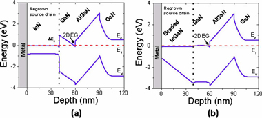
Figure 1: Simulated band diagrams for regrown InN (a) and InGaN graded from GaN to InN (b) source/drain regions for N-polar GaN HEMT.
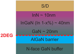 Figure 2. Epitaxial structure of HEMT and re-grown graded InGaN used to lower the contact resistance and to enable high conduction path to HEMT 2DEG.
To achieve these effects, the HEMT has to be grown using N-face (Figure 3) rather than the more usual III-face materials, reversing the polarization direction. The UCSB researchers grew the N-face AlGaN/GaN HEMTs on C-face silicon carbide substrates using plasma-assisted molecular beam epitaxy (PAMBE) and on sapphire (miscut 4° in the a-direction) using metal-organic chemical vapor deposition (MOCVD). This resulted in a 2DEG with carrier density of about 1x10¹³/cm2 and mobility of 1200–1400cm2/V-s.
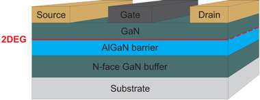
Figure 3: Schematic of N-face GaN HEMT without graded source/drain.
The InGaN re-growth was performed using PAMBE after the tungsten/chromium gate-metal stripes had been deposited, along with a silicon dioxide covering and silicon nitride side-wall spacers. Contacts using pure InN were also produced. Different re-growth temperatures and various grading schemes were used to find the optimum parameters (Table 1). The source/drain contacts consisted of electron-beam-evaporated non-alloyed layers of titanium and gold.
Growth temperature |
Ga flux |
In flux |
InxGa1−xN |
°C |
x10−7Torr |
x10−7Torr |
% |
(a) |
|||
610 |
3–1.5 |
5 |
1–26 |
550 |
2.8–1.5 |
3.2 |
1–35 |
475 |
2.4–1.5 |
2.8 |
1–43 |
(b) |
|||
575 |
3–1.5 |
4.2 |
1–30 |
575 |
3–1 |
4.2 |
1–54 |
575 |
3–0.75 |
4.2 |
1–63 |
Table 1: (a) Final InGaN composition in the grade obtained by varying growth temperature, and keeping end Ga-flux constant. (b) Second grading scheme: growth temperature was kept constant but final Ga-flux was decreased to obtain higher In incorporation and steeper grading profile.
The best contact resistance of 27Ω-μm was obtained with InxGa1-xN graded from an x-value of 0.01 to 0.63 (i.e. from 1% to 63%) grown at 575°C (Figure 4). A HEMT created using this scheme and a 10nm InN cap demonstrated a maximum current of 1.2A/mm and an on-resistance of ~0.9Ω-mm.
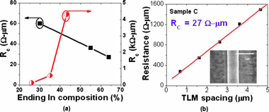
Figure 4: Ohmic contact resistance values for graded InGaN grown at varying growth temperature and InGaN grading as in Table 1.
The researchers say that further characterization of large- and small-signal DC and radio-frequency performance will be reported in the future.
A similar technique — combining N-face polarization with AlGaN, rather than InGaN grading — has recently been used by University of Notre Dame to make ‘three-dimensional hole gases’, increasing hole concentrations and hence hole injection in AlGaN ultraviolet/blue light-emitting diodes [John Simon et al, Science, vol327, p60, 2010; see upcoming report in Mike Cooke, Semiconductor Today, April 2010].
See related items:
Seeking ultra-low ohmic path to high-frequency nitride transistors
Gate control of terahertz transistor emission frequency
Reducing GaN HEMT degradation with InAlN barrier
![]() Search: UCSB InGaN InN AlGaN/GaN HEMTs SiC substrates PAMBE Sapphire MOCVD
Search: UCSB InGaN InN AlGaN/GaN HEMTs SiC substrates PAMBE Sapphire MOCVD
Visit: http://link.aip.org
Visit: http://my.ece.ucsb.edu
The author Mike Cooke is a freelance technology journalist who has worked in the semiconductor and advanced technology sectors since 1997.
![]() ©2010 Juno Publishing and Media Solutions Ltd. All rights reserved. Semiconductor Today and the editorial material contained within it and related media is the copyright of Juno Publishing and Media Solutions Ltd. Reproduction in whole or part without permission from Juno Publishing and Media Solutions Ltd is forbidden. In most cases, permission will be granted, if the author, magazine and publisher are acknowledged.
©2010 Juno Publishing and Media Solutions Ltd. All rights reserved. Semiconductor Today and the editorial material contained within it and related media is the copyright of Juno Publishing and Media Solutions Ltd. Reproduction in whole or part without permission from Juno Publishing and Media Solutions Ltd is forbidden. In most cases, permission will be granted, if the author, magazine and publisher are acknowledged.
Disclaimer: Material published within Semiconductor Today and related media does not necessarily reflect the views of the publisher or staff. Juno Publishing and Media Solutions Ltd and its staff accept no responsibility for opinions expressed, editorial errors and damage/injury to property or persons as a result of material published.
Semiconductor Today, Juno Publishing and Media Solutions Ltd, Suite no. 133, 20 Winchcombe Street, Cheltenham, GL52 2LY, UK
Web site by No Name No Slogan ![]()