| Home | About Us | Contribute | Bookstore | Advertising | Subscribe for Free NOW! |
| News Archive | Features | Events | Recruitment | Directory |
News
15 July 2010
AlN substrate used to make 260–240nm UV LEDs
Crystal IS Inc of Green Island, NY, USA has reported research results for LEDs emitting in the 260–240nm mid- or ‘deep’ ultraviolet (UV) range of wavelengths [James R. Grandusky et al, Appl. Phys. Express, vol3, p072103, 2010]. Unlike other companies producing mid-UV devices, Crystal IS uses high-quality bulk aluminum nitride (AlN) substrates as opposed to growing AlN template layers on sapphire substrates.
Like many researchers in the area, one of the more immediately proposed applications of mid-UV LEDs is for water and air purification. UV radiation in this frequency range has the capability of disrupting biological material such as DNA, killing micro-organisms.
One reason for using AlN substrates is the hope of reducing threading dislocation densities (TDDs) through the active region. Without special measures, such as lateral overgrowth or migration-enhanced/pulsed growth, TDDs on sapphire tend to be in the region of 1010/cm2. More specialized techniques on sapphire can manage to reduce this to 108/cm2.
The impact of high TDDs tends to limit both the efficiency of the resulting devices and reliabilities. External quantum efficiencies (EQEs) for these types of devices are presently limited to about 3% or even less [www.semiconductor-today.com/news_items/2010/JUNE/NAGOYA_140610.htm].
Crystal IS has previously found that pseudomorphic (strained) layers of AlGaN grown on AlN can be grown to greater thicknesses than expected from thermodynamic considerations. AlGaN with 60% Al is expected to have a critical thickness of only 40nm, while Crystal IS managed layer thicknesses of up to 0.5μm without strain relaxation (and hence without TDDs being formed by such relaxation). For 70% Al layers, this thickness increases to 1μm.
These are the sort of thicknesses needed for the underlying n-type contact layers. The latest Crystal IS LEDs (Figure 1) consisted of a silicon-doped n-type Al0.7Ga0.3N layer, a five-period multi-quantum well (MQW) with n-Al0.7Ga0.3N barriers and Al0.55Ga0.45N wells, an n-Al0.8Ga0.2N electron-blocking layer (EBL) and a p-GaN contact.
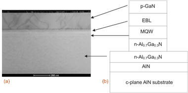
Figure 1: TEM image showing low dislocation density in the active region (a), and corresponding schematic of the device structure (b).
The epitaxial material was formed into 360μm-diameter circular mesas. The n-contact metal consisted of titanium/aluminum/titanium/gold and the p-contact was nickel/gold. The LED wafer was thinned to 200μm thick and the surface roughened to improve extraction.
The material quality was examined using cross-sectional transmission electron micrography (TEM). Although the dislocation density in the pseudomorphic layers below the p-contact is described as ‘low’, including the active MQW, the mismatch between the AlGaN EBL and the thick p-GaN contact was large (~2.4%), creating a TDD above the EBL of around 1010/cm2.
Pulsed and continuous-wave (CW) currents were used to test the output from the device. No heat sink was used, so the pulsed testing (10μsec, 1% duty cycle) was used initially to avoid self-heating effects that can impact efficiency and reliability.
A device with a 248nm emission peak had a full-width half-maximum (FWHM) for the spectrum of 13.9nm at 20mA current and 14.9nm at 300mA. The EQE ranged from 1.44% at 20mA to 1.09% at 300mA. The output power at 300mA was 16.3mW. The high forward voltage of 18V at 300mA is blamed on the difficulties in contact formation and non-optimized device geometry. The researchers say that this problem “is being addressed in future designs”.
The devices have a fast initial decay in performance over several hours, followed by more prolonged degradation. The researchers believe that, since no burn-in period was used, some of the decay in EQE of the 248nm device with increased current can be attributed to this degradation.
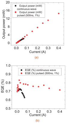 Another device emitting at 243nm was tested using pulsed and CW currents (Figure 2). The peak light output power for CW operation was 2mW, while the pulsed figure was 15mW. The EQE peaked at 30mA and fell quickly, indicating self-heating effects. Under pulsed operation, the fall-off after the peak is much slower (14.6mW output power and 0.72% EQE at 400mA). The smaller drop in EQE compared with the 248nm device is attributed to the burn-in effect of performing CW tests before pulsing.
Figure 2: Output power (a) and EQE (b) vs current for a 243nm device in CW and with a 1% duty cycle and 500ns pulse width.
The wavelength also shifted 23meV under CW operation between 20mA and 70mA, indicating a junction temperature rise of ~57°C. With pulsed operation there was no such shift.
The researchers found relatively consistent performance in devices produced within a wafer and within epi runs. Some 438 dies emitting in the 240–250nm range had a mean output power of 1.1mW under CW operation, with the peak being 5.8mW. For 137 devices emitting at 250–260nm, the mean power was 2.5mW, with a 5mW peak.
The research was funded by a US National Institute of Science and Technology (NIST) Advanced Technology Project (ATP) grant and money from the US Department of Energy (DOE) and the US Army Research Laboratory (ARL).
See related items:
Deep UV LED efficiency reaches 3%
Large chip improvements to deep-ultraviolet output power
First demonstration of semipolar III–nitride ‘deep-UV’ LED
Nichia achieves 2.78% external quantum efficiency for 281nm UV-LED
![]() Search: Crystal IS AlN substrates UV LEDs
Search: Crystal IS AlN substrates UV LEDs
Visit: http://apex.ipap.jp
The author Mike Cooke is a freelance technology journalist who has worked in the semiconductor and advanced technology sectors since 1997.
![]() ©2010 Juno Publishing and Media Solutions Ltd. All rights reserved. Semiconductor Today and the editorial material contained within it and related media is the copyright of Juno Publishing and Media Solutions Ltd. Reproduction in whole or part without permission from Juno Publishing and Media Solutions Ltd is forbidden. In most cases, permission will be granted, if the author, magazine and publisher are acknowledged.
©2010 Juno Publishing and Media Solutions Ltd. All rights reserved. Semiconductor Today and the editorial material contained within it and related media is the copyright of Juno Publishing and Media Solutions Ltd. Reproduction in whole or part without permission from Juno Publishing and Media Solutions Ltd is forbidden. In most cases, permission will be granted, if the author, magazine and publisher are acknowledged.
Disclaimer: Material published within Semiconductor Today and related media does not necessarily reflect the views of the publisher or staff. Juno Publishing and Media Solutions Ltd and its staff accept no responsibility for opinions expressed, editorial errors and damage/injury to property or persons as a result of material published.
Semiconductor Today, Juno Publishing and Media Solutions Ltd, Suite no. 133, 20 Winchcombe Street, Cheltenham, GL52 2LY, UK
Web site by No Name No Slogan ![]()