| Home | About Us | Contribute | Bookstore | Advertising | Subscribe for Free NOW! |
| News Archive | Features | Events | Recruitment | Directory |
News
31 March 2010
Nichia achieves 2.78% external quantum efficiency for 281nm UV-LED
Japan’s Nichia Corp has added its results to the recent wave of published deep ultraviolet (DUV) LED research [Akira Fujioka et al, Appl. Phys. Express, vol3, p041001 2010]. Using an aluminum nitride (AlN) on sapphire template, its researchers produced devices emitting radiation at a wavelength of 281nm with an external quantum efficiency (EQE) of 2.78% at 20mA (2.45mW output power, 7.53V forward voltage).
Nichia is attracted by the recent proposed applications for such devices in disinfection, sensing, and polymer curing. The traditional competitor for such applications is mercury lamps, which require careful handling to avoid the release of dangerous metal vapor. Further advantages of LEDs include lower energy consumption, better robustness, and longer operation before failure.
Researchers are working hard to bring the relatively low external quantum efficiencies (EQEs) of DUV LEDs (less than 2%) nearer to the achievements of visible LEDs (up to 70%). As is often the case with nitride semiconductors, dislocations from the template that thread through epitaxial structures are blamed for the low EQEs. Some groups have adopted special lateral overgrowth techniques to reduce the density of defects on the template surface.
Nichia prefers to follow the simpler suggestion that increasing the AlN layer thickness can reduce the threading dislocation density and improve crystalline quality. It produced flip-chip (FC) structures where the final devices emit the UV light through the sapphire substrate. The emitting region of the device was a multi-quantum well consisting of various layers of aluminum gallium nitride (Figure 1).
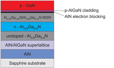
Figure 1: Schematic structure of Nichia’s DUV LED.
An undoped 1nm AlN electron blocking layer (EBL) was used to reduce the number of electrons reaching the magnesium-doped p-type region, since recombination there tends to be non-radiative or of longer wavelength. A further problem for the p-type contact is that is constructed from 300nm GaN that absorbs 281nm radiation, since its photons exceed the bandgap energy of 3.4eV. Nichia attributes its EQE of more than 2% to the use of high-quality AlN templates, the AlGaN MQW structure, and EBL.
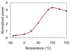 Figure 2: Temperature dependence of normalized output power from –40°C to 150°C.
In DC operation, the new Nichia devices actually produced more output power, achieving maximum power after about a minute. This effect was probably due to self-heating ionizing the acceptor doping in the p-type region, releasing holes (thermally enhanced p-type activation). Indeed, studies of the temperature dependence of the device (Figure 2) suggest that it is most efficient around 100°C. Using pulsed currents (50μsec width, 2kHz repetition), the output power was 0.69mW (28% that achieved with DC operation). Nichia believes that further effort to improve activation of the p-type layers is required for superior LED characteristics.
An arrangement of 26 LEDs (2x13) produced an output of 223mW with pulse injection (5ms, 10Hz repetition) at 1.85A. The aim of this was to demonstrate the feasibility of constructing LED-based high-power UV sources. Measurements were carried out with water cooling. The maximum current was limited by the ability to remove heat from the devices across the bonding interface between the LED chip and sub-mount. The maximum current in DC operation was 460mA (~35mA/die), giving a UV output of 60mW.
The structures were grown using low-pressure metal-organic chemical vapor deposition with simultaneous trimethyl-metal and ammonia (NH3) sources. The deposition did not use any special techniques such as migration enhancement or pulsing. The thickness of the base AlN layer was 3μm and x-ray diffraction analysis gave rocking curve full-width at half maximum (FWHM) values of 60arcsec and 600arcsec for the 002 and 102 crystal planes. The typical 102 FWHM for 1μm AlN layers is more than 1000arcsec. After the AlN template, an AlN/AlGaN superlattice was used to relieve strain arising from lattice mismatches before depositing the silicon-doped n-type contact layers (0.5μm undoped, 2.5μm doped). A 50nm electron supply layer also served as the first barrier of the MQW structure (two pairs of 4nm Al0.45Ga0.55N wells and 2.5nm Al0.56Ga0.44N barriers).
The contacts to the n-type regions consisted of titanium/aluminum and, for the p-type regions, indium tin oxide (ITO). The package was a wire-bonded TO-18 casing with no encapsulation.
See related items:
Increased UV power from diamond LEDs enables E. coli sterilization
Multi-quantum blocking raises deep-UV LED efficiency
Improving deep UV emission on aluminum nitride templates
Deep ultraviolet power boost at shorter wavelengths
Visit: http://apex.ipap.jp/link?APEX/3/041001
The author Mike Cooke is a freelance technology journalist who has worked in the semiconductor and advanced technology sectors since 1997.

![]() ©2010 Juno Publishing and Media Solutions Ltd. All rights reserved. Semiconductor Today and the editorial material contained within it and related media is the copyright of Juno Publishing and Media Solutions Ltd. Reproduction in whole or part without permission from Juno Publishing and Media Solutions Ltd is forbidden. In most cases, permission will be granted, if the author, magazine and publisher are acknowledged.
©2010 Juno Publishing and Media Solutions Ltd. All rights reserved. Semiconductor Today and the editorial material contained within it and related media is the copyright of Juno Publishing and Media Solutions Ltd. Reproduction in whole or part without permission from Juno Publishing and Media Solutions Ltd is forbidden. In most cases, permission will be granted, if the author, magazine and publisher are acknowledged.
Disclaimer: Material published within Semiconductor Today and related media does not necessarily reflect the views of the publisher or staff. Juno Publishing and Media Solutions Ltd and its staff accept no responsibility for opinions expressed, editorial errors and damage/injury to property or persons as a result of material published.
Semiconductor Today, Juno Publishing and Media Solutions Ltd, Suite no. 133, 20 Winchcombe Street, Cheltenham, GL52 2LY, UK
Web site by No Name No Slogan ![]()