- News
8 December 2011
Triode probe of efficiency droop in nitride semiconductor light emitters
Researchers in South Korea and USA have used nitride semiconductor light-emitting triode structures (LETs) to investigate the effect of hole injection on light output [Sunyong Hwang et al, Appl. Phys. Lett., vol99, p181115, 2011]. The work was carried out by South Korea’s Pohang University of Science and Technology (POSTECH) and Rensselaer Polytechnic Institute (RPI) of Troy, NY, USA.
Hole injection is known to be particularly poor in nitride semiconductor light-emitting diodes (LEDs) and has been blamed for the ‘efficiency droop’ effect by some groups. ‘Efficiency droop’ describes the fall-off in efficiency of nitride LEDs as the injection current is increased. Many other causes have been suggested for the effect, including device heating, Auger recombination, delocalization of carriers from indium-rich low-defect-density regions, and electron leakage.
The POSTECH/RPI structure (Figure 1) consists of two anodes and a cathode. The anodes consisted of inter-digitated metal structures on the p-type contact layer. The connection to the n-type layer formed the cathode.
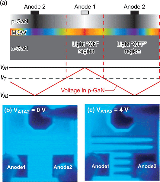
Figure 1: (a) Effective area modulation of the active region of an LET with a linear voltage variation approximation. Top view of the lit-up LETs under different anode-to-anode voltages: (b) 0V and (c) 4V.
The two anodes are used to accelerate the holes in the p-type layers, giving them kinetic energy. The extra kinetic energy raises the effective temperature of the holes above that of the crystal lattice, easing their passage over the hole barrier of the electron-blocking layer (EBL). The electric field between the 8μm-spaced anodes can reach ~104V/cm at moderate bias.
The POSTECH/RPI researchers used a typical blue (450nm wavelength) LED structure grown on c-plane sapphire using metal-organic chemical vapor deposition (MOCVD). The active layer consisted of a 6-period multi-quantum well (MQW) with 3nm undoped GaInN in the wells and 9nm n-GaN barriers. The electron-blocking layer consisted of Al0.15Ga0.85N.
The LET consisted of a mesa produced through inductively coupled plasma (ICP) etch and deposition and annealing of ohmic contacts (n-type/cathode, titanium/aluminum/titanium/gold; p-type/anodes 1 and 2, nickel:zinc/silver).
Efficiency measurements were carried out with increasing bias between the anodes (VA1A2). Although the droop decreases with increasing anode bias, the peak efficiency also declines. The researchers explain this result as being due to the reduced area of light emission due to different anode potentials placing only part of the device above the threshold voltage of 2.86V, giving 1mA current from the n-type layer for the particular structure used (Figure 1).
By correcting for the reduced effective area modulation (EAM) of light emission, the researchers give a series of curves showing increased efficiency against current density with increasing bias between the anodes (Figure 2). The increased efficiency is attributed to higher hole injection enabled by the LET structure. The researchers also note that higher bias leads to a slower decline in efficiency with increasing current density, concluding: “This trend indicates that the limited hole-injection efficiency is one of the major causes of the efficiency droop in GaN-based LEDs.”
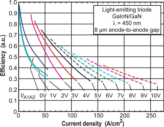
Figure 2: Efficiency versus drive current density for LETs under different anode-to-anode biases, as corrected for effective area modulation (EAM) of light emission.
Financial support for the work came from South Korea’s Industrial Technology Development Program funded by the Ministry of Knowledge Economy (MKE) and Priority Research Centers Program of the National Research Foundation of Korea (NRF).
Grading barriers for improved hole transport
Reducing LED droop at high current with nitride semiconductors
UCSB theory blames indirect Auger recombination for nitride LED droop
Exploring droop and wide-well nitride LEDs
LEDs Efficiency droop MOCVD GaN AlGaN
http://link.aip.org/link/doi/10.1063/1.3658388
The author Mike Cooke is a freelance technology journalist who has worked in the semiconductor and advanced technology sectors since 1997.