- News
31 May 2011
Nitrogen-polar advantages for longer-wavelength nitride LEDs
Ohio State University (OSU) researchers have used a new growth model for nitrogen-polar (N-polar) nitride material to create 540nm (green) light-emitting diodes (LEDs) at 600°C using plasma-assisted molecular beam epitaxy (PAMBE) [Fatih Akyol et al, Jpn. J. Appl. Phys., vol50, p052101, 2011]. One of the researchers is also affiliated with Turkey’s Atatürk University.
N-polar growth is quite widely used in the development of nitride semiconductor electronic devices and has achieved comparable performance to gallium-polar (Ga-polar) devices. This has not been the case so far for optoelectronic devices.
In the case of long-wavelength light-emitting devices, it is hoped that, by reversing the direction of the polarization field in nitride semiconductor devices, performance and growth parameters can be changed beneficially.
To increase the wavelength into the green part of the visible spectrum, one needs increasing amounts of indium in the nitride semiconductor alloy. Unfortunately, indium nitride (InN) has a much lower optimal growth temperature than the gallium nitride (GaN) it is being alloyed into.
Also, the two materials have a different lattice constant, so the InGaN layers are strained compared with the background GaN lattice, leading to large strain-dependent (piezoelectric) polarization fields.
These factors make it difficult to grow high-quality InGaN multi quantum well (MQW) structures.
N-polar InN can be grown at temperatures about 100°C higher than with Ga-polar growth using PAMBE. It is believed that this is because InN has higher stability on N-polar surfaces. Inspired by this, the OSU group has recently grown InGaN at ‘significantly higher’ temperatures than usual by growing in the N-polar direction.
 In addition, the high polarization fields can lead to poor carrier confinement in the active region of light-emitting devices. Normal growth techniques on c-plane GaN templates lead to crystal structures oriented with a Ga-face surface. Orienting in the opposite N-polar direction reverses the spontaneous and piezoelectric polarization fields, which can be advantageous in terms of carrier confinement and thus device performance.
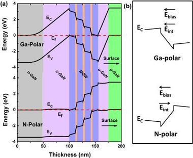
Figure 1: (a) Schrödinger–Poisson computation of energy band diagrams of typical InGaN MQW device with both polarities, including spontaneous and piezoelectric polarization. (b) State of the intrinsic (including both spontaneous and piezoelectric polarization) and bias-induced electric fields in the QWs of a typical device in both polarities.
One effect is that the polarization field then acts in the direction of the depletion of the p–n junction structure, reducing the depletion width (Figure 1). This is in contrast to Ga-polar devices, where the polarization field points in the opposite direction, increasing the depletion width. The reduced depletion width is expected to reduce turn-on voltages for light-emitting devices.
Another effect is that, under bias, the polarization field and bias field tend to act against each other in N-polar devices. This means that there is less tendency for the electrons and holes to separate (quantum-confined stock effect, QCSE), unlike in Ga-polar devices. Electron–hole separation reduces light-emission probabilities.
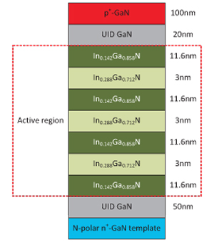 The OSU researchers used an N-polar free-standing LED-quality GaN template (dislocation density ~108/cm2) from Lumilog in France. The growth was carried out using RF PAMBE. During the multi quantum well (MQW) growth (Figure 2) the gallium and indium fluxes were kept constant with an In-rich environment, leading to In-coverage of the surface. The InGaN composition for wells and barriers was controlled by the nitrogen flux. The growth temperature was 600°C.
Figure 2: Epitaxial design of the green MQW LED.
The p-contact consisted of nickel-gold-nickel. Inductively coupled plasma (ICP) etching was used to create mesas down to the n-type layer, where a titanium-gold contact was deposited. The device area was 17,000μm2. Measurements were carried out at room temperature using continuous-wave (cw) operation.
The turn-on voltage of the device was 5V with differential resistance of 72Ω (0.012Ω-cm2). Some variation in light intensity was found across the contact, which was attributed to unoptimized growth of the p-GaN layer and ohmic contacts.
The performance was tested up to 30mA, corresponding to 176A/cm2 density (Figure 3). The researchers describe the increase in electroluminescence as ‘linear’ up to 88/A/cm2 (15mA), beginning to saturate after this, due to self-heating effects on the device operation.
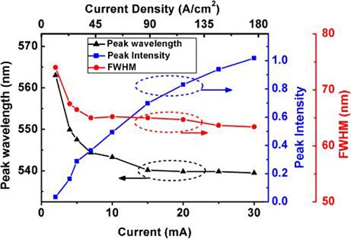
Figure 3: EL emission peak intensities (normalized to the highest value), peak wavelengths and FWHMs as a function of driving current from 2mA to 30mA (11A/cm2 to 176A/cm2).
The blue-shift between 2mA (563nm) and 30mA (540nm) was 23nm, attributed to screening of the piezoelectric field by electrons and holes at higher injection current density. The blue-shift between 15mA and 30mA was only 0.7nm. The much smaller blue-shift in this range is again attributed to self heating, with the higher junction temperature reducing the energy bandgap, in competion against ‘band-filling effects’, where the energy levels fill up at higher currents, widening the energy difference between electrons and holes.
The spectral peak full-width at half maximum (FWHM) value was wider than with state-of-the-art green LEDs. “The growth conditions used for the LEDs described in this work were optimized only to achieve the required emission wavelength,” the researchers explain. They believe that fluctuations in indium and quantum well thickness contribute to their FWHM results.
Sapphire patterning boosts green light generation and extraction
UCSB uses more uniform InGaN for record efficiency semi-polar green LED
Ohio boosts nitride tunneling current to 118A/cm2 at –1V
Green LEDs N-polar InN GaN PAMBE Lumilog
The author Mike Cooke is a freelance technology journalist who has worked in the semiconductor and advanced technology sectors since 1997.