- News
7 December 2011
Increasing performance with III-V transistors on silicon
A first demonstration of a new metal source/drain technology for extremely thin body (ETB) indium gallium arsenide (InGaAs) transistor channels on insulator (OI) with silicon substrates has been reported by University of Tokyo, National Institute of Advanced Industrial Science and Technology and Sumitomo Chemical Co Ltd [SangHyeon Kim et al, Appl. Phys. Express, vol4, p114201, 2011].
ETB-OI devices with channel mobilities as high as 1700cm2/V-s were produced, despite the channel being only 10nm thick. Although the mobility was much reduced in 5nm-thick channel devices, other parameters improved, such as the on/off current ratio increasing to 105 and the subthreshold swing being reduced to 120mV/dec.
These achievements were due to the use of a new self-aligned source–drain technology involving nickel-indium gallium arsenide alloys reported by the same research collaboration earlier this year [see Self-aligned Ni-InGaAs as source–drain for InGaAs MOSFET or Semiconductor Today, p104, February 2011]. The technology avoids the damage of traditional ion implant doping and allows the use of light doping of the channel. High doping and ion damage increase resistance, reducing transistor performance.
The researchers produced the new devices (Figure 1) using direct wafer bonding (DWB) techniques. The p-type layers of In0.53Ga0.47As (5nm) or In0.7Ga0.3As (10nm) were grown on 2-inch indium phosphide (100) substrates using metal-organic chemical vapor deposition (MOCVD). The acceptor concentration was ~1016/cm2.
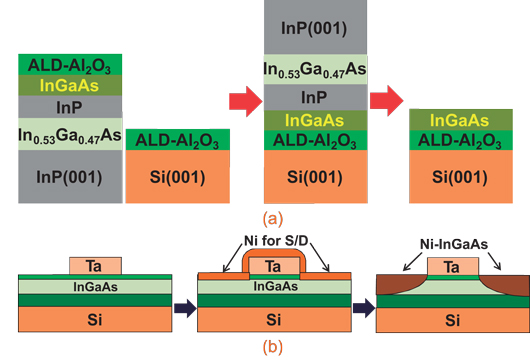
Figure 1: Fabrication of (a) III–V-OI on Si substrate by DWB and (b) InGaAs-OI MOSFETs with metal S/D structure using Ni–InGaAs alloy.
The InP substrate had sacrificial layers of In0.53Ga0.47As and InP before the channel, for use in a subsequent series of wet etch processes involving hydrochloric acid and a mix of phosphoric acid and hydrogen peroxide. The wet etches were performed after bonding to the silicon substrate (n+, (100)). Wet etch was chosen so that the ETB In0.7Ga0.3As or In0.53Ga0.47As channel layer was smooth and uniform with a root mean square surface roughness ~0.55nm.
The bonding was achieved by first passivating with ammonium sulfide ((NH4)2S) solution and applying aluminum oxide (Al2O3) insulator with atomic layer deposition (ALD) at 200°C on the InGaAs and Si surfaces. The bond was carried out in air after a 330°C pre-bond anneal.
The gate dielectric consisted of 10nm of Al2O3 deposited by ALD. The gate electrode metal was tantalum (Ta). The source/drain electrodes were produced with Ni-InGaAs alloy: first, nickel was deposited on the S/D regions and annealed at 250°C for a minute to make the alloy with InGaAs; then, unreacted nickel was removed using hydrochloric acid for three minutes. Finally, aluminum electrode pads were deposited and the devices were isolated by etching a 10μm gap.
In0.7Ga0.3As 10nm-thick channel devices with 5μm gate length and 150μm width had transfer characteristics that are described as “good” by the researchers, although the subthreshold swing of 347mV/dec is “quite high”.
In fact, one would want to see a much lower value for this parameter: a number of groups have achieved 120mV/dec and better with III-V devices, and one would even then want to get closer to the 60mV/dec theoretical limit for planar devices. Traditional silicon CMOS can reach below 100mV/dec.
The researchers explain their high swing value as arising possibly from a large off-leakage current due to the InGaAs layer remaining between the active region of the MOSFET and the isolation mesa edge.
The drain current saturation and pinch-off characteristics are good (i.e. flat). There is a shift in threshold between a drain bias of 50mV and 1V, indicating the effect of drain induced barrier lowering, due to either large source/drain parasitic resistance and/or the large off-state leakage current.
The parasitic S/D resistance of 38.2kΩ-μm also gives a low on-current, with an on-resistance of 45kΩ-μm ((1V)/(22μA/μm)). This high resistance is attributed to the thinness of Ni-InGaAs alloy layers and the long distance from the channel to the electrode pad metal contacts.
New devices with lightly doped In0.7Ga0.3As and In0.53Ga0.47As 10nm channels were compared with previous heavily doped 9nm In0.53Ga0.47As channel devices. The previous devices were produced by the same collaboration and reported last year.
Lead researcher SangHyeon Kim comments: “Our previous work used an n-type channel because there was a difficulty in the formation of S/D (ion implantation, etc) with the ETB-OI structure. Therefore, we then fabricated InGaAs-OI with highly n-type doped channel (fabricated using in-situ doping during epitaxial growth). Its operation was similar to that of depletion type MOSFETs (junctionless transistor). However, this type of device has a lot of dopant in the channel, causing reduced mobility.
“In our new work, we have introduced (could introduce) a lightly doped p-type channel using the novel S/D formation method (metal S/D). This new device is an inversion-type MOSFET that operates in a similar way to silicon CMOS transistors. Despite the different depletion- and inversion-modes of operation, both devices use electrons as channel carrier in the on-state.”
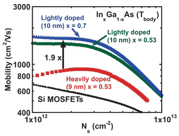 The reduction in doping from an donor concentration (ND) of 1019/cm3 to an acceptor concentration (NA) of 1016/cm3 gave an enhancement in mobility of up to 1.9x with an inversion carrier density 1012/cm2 (Figure 2). This improvement is attributed to reduced carrier scattering from ionized acceptors.
Figure 2: Mobility characteristics of the heavily doped (ND ~ 1019/cm3) 9-nm-thick In0.53Ga0.47As-OI channel and lightly doped (NA ~ 1016/cm3) 10-nm-thick InxGa1- xAs-OI MOSFETs (x ~ 0.53 and 0.7).
For the In0.7Ga0.3As device, the mobility was 1700cm2/V-s at this inversion carrier density. All the InGaAs devices had higher mobility than Si-based devices over the inversion carrier density range 1012-1013/cm2.
The researchers also produced devices with 5nm thick In0.7Ga0.3As channels. At drain bias 1V, the on-off current ratio was 105 and the subthreshold swing was reduced to 120mV/dec. The off current was as small as 5pA/μm.
The 5 orders of magnitude improvement in off current is ascribed to the likely increase in effective band gap due to stronger quantization and/or effective reduction in possible leakage passing through the InGaAs layer that remains between the active region of the MOSFET and the isolation mesa edge due to such a low body thickness.
Unfortunately, the on-current is also reduced with the thinner channel. This is attributed to mobility degradation and increased series resistance. The series resistance of the 5nm channel was 442.6kΩ-μm, compared with the 38.2kΩ-μm of the 10nm channel. The mobility was also reduced to less than 100cm2/V-s for the range 1012-1013/cm2 of inversion carrier density.
The researchers point to recent reports on the effects of surface roughness and dielectric deposition on device performance. Roughness reduction and process optimization can therefore be expected to deliver better performance in the future.
Self-aligned Ni-InGaAs as source–drain for InGaAs MOSFET
Power, speed and other highlights of IEDM 2010
Capacity of InGaAs to increase drive current in nano MOSFETs
The author Mike Cooke is a freelance technology journalist who has worked in the semiconductor and advanced technology sectors since 1997.