- News
4 February 2011
Self-aligned Ni-InGaAs as source–drain for InGaAs MOSFET
Researchers in Japan have developed a self-aligned nickel-indium gallium arsenide (Ni-InGaAs) alloy source/drain (S/D) process for application in InGaAs n-type metal-oxide-semiconductor field-effect transistors (nMOSFETs) [SangHyeon Kim et al, Appl. Phys. Express, vol4, p024201, 2011]. The scientists are variously based at University of Tokyo, National Institute of Advanced Industrial Science and Technology (NAIST), Sumitomo Chemical Co Ltd.
The self-aligned process is seen as an important potential ingredient of a manufacturable device. Silicon complement MOSFET (CMOS) processes presently use a self-aligned silicide (‘SAlicide’) S/D process. The self-alignment refers to using previously patterned structures rather than a separate lithographic process (that would require precise alignment) to form the S/D contact regions.
InGaAs devices are being developed with a view to enhancing the performance of the CMOS logic circuits that are at the base of present day electronics. In particular, as these devices become smaller, the electronic properties of silicon are not sufficient to overcome a series of ‘short-channel effects’. InGaAs is attractive because it has a much higher mobility than silicon (but also has other problems that are being intensively worked on by researchers).
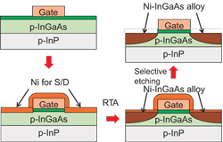 The Tokyo/NAIST/Sumitomo process starts with metal-organic chemical vapor deposition (MOCVD) of p-type InGaAs on indium phosphide substrates (Figure 1). This is followed by atomic layer deposition (ALD) of 10nm aluminum oxide (Al2O3) insulating material. A nickel gate is then formed by electron-beam deposition and lithographic patterning.
Figure 1: Fabrication process for InGaAs MOSFET with self-aligned metal S/D structure.
After the gate has been formed, a further 30nm of nickel is deposited to create the S/D regions. Ni-InGaAs alloying is achieved through a rapid thermal anneal at 250°C for 1 minute. Hydrochloric (HCl) acid solution was used to remove unreacted Ni, leaving just the Ni-InGaAs alloy.
Aluminum metal was used for the S/D electrodes. A back contact electrode of gold-zinc was also applied.
The device had a gate length of 5μm and a width of 150μm. These figures are a way off from today’s 32nm (~ 5μm/150) technology and future devices seeking gate lengths less than 18nm.
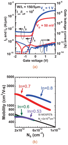 With an In0.7Ga0.3As channel (Figure 2a), the device achieved on/off current ratio of 104 and subthreshold slope of 147mV/dec (a low figure indicates a desirable sharp turn-on of current). Other III-V devices have achieved 120mV/dec and better. Silicon CMOS achieves around 70mV/dec.
Figure 2: (a) ID and IS versus VG characteristics of an In0.7Ga0.3As MOSFET with self-aligned metal S/D. (b) Electron mobility versus the channel electron sheet density (NS) characteristics in InxGa1-xAs MOSFETs. The Si electron mobility is also shown. The enhancement for InGaAs over Si is up to 3.8x at NS of 8x10¹²/cm2.
Before producing MOSFETs, the Tokyo/NAIST/Sumitomo team characterized Ni-InGaAs as an S/D material. This meant finding ways to reduce its sheet resistance and its Schottky barrier height with the InGaAs channel.
The researchers performed a rapid thermal anneal (RTA) of Ni on InGaAs over a range of temperatures, finding that above 250°C a Ni-InGaAs alloy is formed with a sheet resistance of around 25Ω/square. The ability to use RTA in such a way to create Ni-InGaAs is reported as ‘a new finding’. This is around a third of the value of maximum conductivity n-type InGaAs (~80Ω/square).
Transmission electron microscopy (TEM), transmission electron (TED) and x-ray (XRD) diffraction were used to study the crystal properties of the alloy. Higher RTA temperatures were found to result in structures with a smaller lattice constant.
In order to operate as S/D material, Ni-InGaAs alloy needs to make ohmic contact with the p-type InGaAs channel. The researchers studied the electrical properties of Schottky diode formations of Ni-InGaAs alloy on n- and p-type InGaAs with various In contents (In = 40%, 53%, 60%, 70%, 80%). Schottky diode behavior was weakest at the higher indium concentrations, and temperature dependence studies extracting the Schottky barrier height revealed that the barrier was zero above 70% In.
The researchers produced a number of MOSFETs with different In content channels (53% and above), along with controls with n-type InGaAs S/D regions. The S/D resistances of the various devices were 38.7, 17.6, 5.72 and 2.73kΩ-μm for InGaAs channels with In contents of 53%, 60%, 70% and 80%, respectively. The S/D resistance of the best devices is about a fifth of that for the control devices. The mobilities were also determined (Figure 2b), with the 70% and 80% devices respectively achieving peak values of 2000 and 1810cm2/V-s. The researchers suggest that Schottky barrier effects (increasing the S/D resistance) reduce the effective mobility values for InGaAs channels with lower In content.
Power, speed and other highlights of IEDM 2010
Capacity of InGaAs to increase drive current in nano MOSFETs
First InGaAs FinFETs suppress short-channel effects
Mid-decade timescale for compound/silicon semiconductor integration
The author Mike Cooke is a freelance technology journalist who has worked in the semiconductor and advanced technology sectors since 1997.
Join Semiconductor Today's group on LinkedIn