


News: Microelectronics
2 April 2020
Ozone precursor for hafnium dioxide dielectric in gallium nitride transistors
North Carolina State University in the USA has been studying ozone (O3) as a means to improve hafnium dioxide (HfO2) dielectric deposition for aluminium gallium nitride (AlGaN)-barrier metal-oxide-semiconductor heterostructure field-effect transistors (MOS-HFETs) on silicon substrate [Faisal Azam et al, IEEE Transactions on Electron Devices, vol.67, p881, 2020]. Such devices are being developed for high-voltage/high-frequency power switching and amplification for microwave transmission.
The researchers used AlGaN/GaN epitaxial material on <111> silicon, supplied by NTT Advanced Technology Corp in Japan. The device was fabricated using a single dielectric for both gate insulation and surface passivation of the source/drain access regions, much simplifying the processing (Figure 1).
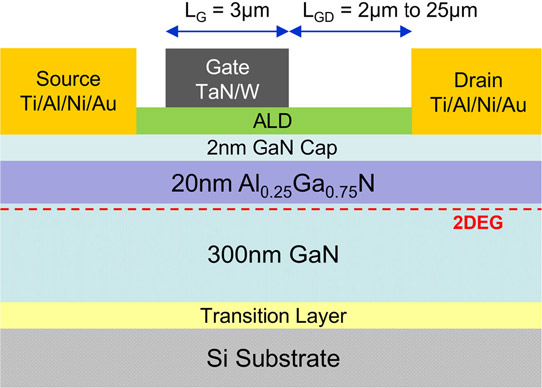
Figure 1: Schematic cross section of AlGaN/GaN MOS-HFET.
The fabrication sequence was: mesa reactive-ion etch, deposition and annealing of titanium/aluminium/nickel/gold (Ti/Al/Ni/Au) source-drain electrodes, ultrasonic and wet surface cleaning of gate and access regions, atomic layer deposition (ALD) of hafnium dioxide (HfO2) gate/passivation dielectric, post-deposition annealing in nitrogen, and radio-frequency sputtering of tantalum nitride/tungsten (TaN/W) gate electrode.
The HfO2 ALD process used tetrakis(dimethylamino)hafnium (TDMAH) as the Hf precursor. For the oxygen component, the team studied the benefits of ozone (O3) over the more usual water (H2O). In capacitance-voltage measurements at 10kHz on MOS structures, the effect of using O3 was to reduce threshold hysteresis by about a factor of two.
The team comments: “The hysteresis is attributed to the trapping and detrapping of charges related to film defects that slowly respond to a voltage sweep. It was also reported that the AlGaN surface might be effectively passivated by supplying only O3 without inducing damage, which leads to improved interface quality.”
The use of O3 oxidation also tended to shift the threshold from around -12V, for H2O precursor, to -6V, depending of ALD process details. This might be related to H+ ions, i.e. protons, being incorporated in the AlGaN surface. Such an effect was absent with O3.
The researchers also varied the ALD process, alternating the HF precursor with either a single- or double-pulse of oxidant. The single-pulse process for O3 resulted in a slightly higher capacitance above threshold, compared with the double O3-O3 pulse ALD recipe. The researchers suggest that this could be due to variation in thickness of the dielectric layer, or change in dielectric constant with the degree of crystallinity, in the two cases.
The MOS-HFETs reached 340mA/mm maximum saturation drain current with O3 dielectric, compared with 240mA/mm for H2O oxidation. The gate potential was 4V. The higher value for O3 dielectric was attributed to a cleaner HfO2/AlGaN interface with less surface states affecting the two-dimensional electron gas (2DEG) used as conduction channel.
The specific on-resistance with the gate at 3V over pinch-off was reduced by 20% from using O3 oxidation in a device with 15μm gate-drain distance. “This is a significant enhancement in the performance that should directly translate to lower conduction loss, i.e. higher efficiency in power-switching applications,” the team writes.
The threshold voltages for devices with H2O, O3 and no (i.e. a Schottky HFET) dielectric were -12.1V, -4.7V and -2.95V, respectively. The more negative threshold for H2O dielectric is again blamed on proton incorporation in the AlGaN barrier. “The additional surface charge at the HfO2/AlGaN interface decreases the voltage drop across the AlGaN barrier layer, thus increasing the threshold voltage,” the researchers explain.
The O3 oxidant also benefited transconductance, giving a peak value of 112.6mS/mm, compared with 81.38mS/mm for H2O-based dielectric. The transconductance boost is said to come from reduced carrier scattering in the channel, due to a lower interface trap density.
Gate leakage was also reduced by more than an order of magnitude by using an O3 ALD process: 5.4x10⁻⁶A/cm2, compared with 1.7x10⁻⁴A/cm2 when H2O oxidant was used. Factors in the improvement were a cleaner interface and higher bulk material quality.
Studies of the effect of temperatures up to 200°C on device performance also showed greater stability of on-resistance and threshold voltage in the O3 ALD devices. The team explains: “The effect of traps exacerbates at elevated temperatures. Hence, it is important for a transistor to start with a cleaner surface, as provided in the case of O3 oxidant, in order to avoid the repercussions of hot-electron effects and traps with increasing temperature.”
High-temperature reverse-bias stress testing was carried out for 1000s at 150°C with 150V drain bias and the gate at 3V below threshold. The Joint Electron Device Engineering Council (JEDEC) standard for indicating 10 year reliability of devices is 1000-hour testing under such conditions. Even for the shorter test period there was a significant contrast in the performance of the H2O and O3 ALD dielectric devices.
The H2O transistors showed a +2.5V drift in threshold (VTH) over the test period. The O3 dielectric reduced this to less than 0.5V. The team comments: “The variation in VTH corresponds to the reduction of the 2DEG in the channel. These results clearly portray that using ozone oxidant is effective both in reducing the HfO2/AlGaN interface states and improving the electrical reliability properties of the MOS-HFETs.”
The current collapse recovery was assessed by applying short pulses with 100ns rise time (Figure 2). The O3 devices performed significantly better than H2O or bare Schottky HFETs. “Specifically, H2O oxidant took 20ms to achieve 90% drain current recovery, whereas O3 oxidant took ~0.1ms to achieve 90% drain current recovery, an extraordinary 200x potential improvement,” the team reports. The reduced interface trap density is credited with the performance recovery.
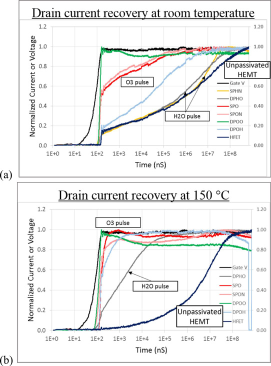
Figure 2: DC/RF dispersion: gate lag at (a) room temperature and (b) elevated temperature, 150°C.
The reduced current collapse of the O3 and H2O oxidant devices, compared with the unpassivated Schottky HFET, was maintained at 150°C high temperature. Indeed, the passivated devices showed reduced current collapse, while the Schottky HFET’s performance worsened further. The higher temperature, it is thought, can enhance detrapping, releasing electrons and restoring the current flow.
In fact, devices where the O3 was applied in two pulses between the Hf pulse in the ALD process showed “near-ideal behavior”, according to the researchers. The team also suggests: “encapsulating the access region and gate with thicker passivation, such as PECVD SiO2 or SiN, we would achieve better gate-lag”.
The researchers explain: “H2O or hydroxyl group (OH-) tends to be strongly physisorbed on all surfaces of the ALD reactor. Since O3 is a stronger oxidizer than H2O, the surface reaction is complete with lower impurity contents and ligands terminated. With a double-pulse, the oxygen vacancies and the hydrogen terminations left behind can be even more effectively filled with repeated exposure to oxygen molecules.”


