


News: Microelectronics
16 April 2020
Magnesium thermal diffusion for normally-on gallium nitride transistors
South China University of Technology has developed a simplified fabrication process for normally-off aluminium gallium nitride (AlGaN)-barrier GaN-channel high-electron-mobility transistors (HEMTs) with p-type gate stack [Lijun Wan et al, Appl. Phys. Lett., vol116, p023504, 2020]. The p-type doping under the gate electrode was achieved by magnesium (Mg) thermal diffusion rather than the more usual inclusion as a precursor in the epitaxial material growth process.
The team comments: “The presented technique is commercially promising in the manufacturing of normally-off HEMTs with outstanding low gate leakage performance.”
The method successfully increased the threshold voltage into positive values, creating a normally-off device, as desired for decreased power consumption and fail-safe operation in high-voltage power switching circuits. Also, the normally-off mode simplifies gate-driver circuit design.
Without special measures, the two-dimensional electron gas (2-DEG) channel that forms near the AlGaN/GaN interface conducts when the gate potential is 0V, giving a normally-on mode
The device was based on epitaxial material with 4.7μm buffer, 300nm undoped GaN channel, 15nm Al0.15Ga0.85N barrier, and 2nm GaN cap layers on silicon.
The transistor fabrication began with 5s inductively coupled plasma (ICP) etch in the gate region, before depositing a 50nm layer of Mg with electron-beam evaporation. The underlying AlGaN was p-type doped with the Mg by rapid thermal annealing at 600°C for a minute. Further annealing in air at 250°C for a minute created a magnesium oxide (MgO) passivation layer.
The source-drain ohmic contacts consisted of annealed titanium/aluminium/nickel/gold. Mesa etching with ICP formed the electrical isolation of the devices. A nickel/gold gate electrode on the MgO completed the transistor.
The rapid ICP etch before Mg deposition roughens the surface and introduces defects, allowing the metal atoms to penetrate/diffuse more deeply into the AlGaN barrier layer in the gate region during the thermal anneal. Atomic force microscopy suggested that the etch depth was around 6nm, removing the GaN cap and partially etching the AlGaN.
Three device types were tested (Figure 1): A was a conventional HEMT without ICP etch or Mg diffusion; B was a HEMT with ICP etch, recessing the gate, but no Mg in the gate region; and, finally, C had the full gate stack with ICP etch and Mg diffusion.
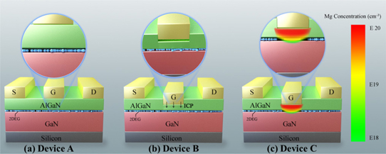
Figure 1: Schematics of (a) bare-bones as-grown device A, (b) device B with etched recessed gate, and (c) device C with Mg diffused gate stack after etching treatment.
The threshold voltages for transistors A-C, in order, were -1.5V, -0.4V, and +1.4V. The corresponding peak transconductances were 68mS/mm, 105mS/mm, and 97mS/mm. In short, the gate stack process transformed the normally-on A transistor into a normally-off device, as desired. Although the gate control, as represented by the peak transconductance, fell back somewhat for device C, the value was still higher than for the bare-bones HEMT A.
The process did hit the drain saturation current from 275mA/mm and 300mA/mm for devices A and B, respectively, with C only managing 173mA/mm. The gate potential in these measurements was +3V. The researchers comment: “The lower saturation current may be caused by the decrease in 2-DEG which is depleted by the holes injected from the Mg-diffused layer.”
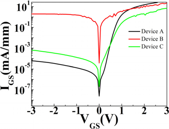
Figure 2: Gate current density (IGS) as function of voltage (VGS) for devices A-C.
The gate leakage currents with 0V gate were 3.7x10⁻⁵mA/mm and 2x10⁻⁷mA/mm for devices B and C, respectively (Figure 2). Transistor C still had only 6.5x10⁻⁴mA/mm gate leakage with the gate at +0.4V. The researchers credit the passivating effect of MgO on surface traps states from the etch processing for the good performance.
Magnesium thermal diffusion GaN HEMTs AlGaN
https://doi.org/10.1063/1.5134918
The author Mike Cooke is a freelance technology journalist who has worked in the semiconductor and advanced technology sectors since 1997.


